Specifications for the voltage regulators (VRs) continue to change to be more and more challenging
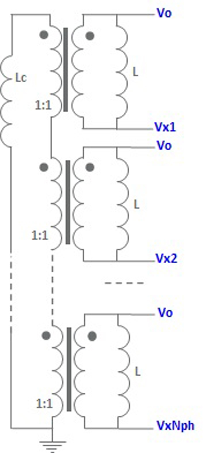
Figure 1: TLVR schematic
Since TLVR is a relatively new development, particular details and properties are still being studied. This article focuses on the transient behavior of TLVR, which affects isolation requirements for the magnetics, as well as isolation and safety considerations for the whole motherboard.
TLVR and Transient
The schematic of TLVR, shown in Fig.1, is used in multi-phase buck regulators. While the main inductor windings are still connected between switching nodes of the phases and Vo, the added auxiliary windings are electrically connected in series to each other and the tuning inductor, LC. Removing LC returns the circuit to just discrete inductors in the buck converter. Shorting LC implies the strongest linking between the phases, as well as the fastest transient performance, but it degrades the current ripple and efficiency.
A potential concern during TLVR transient is the fact that all auxiliary windings are connected in series, with a typical 1:1 transformer ratio-to-primary windings. As the buck phases are typically enabled to align during the transient to improve performance: voltage pulses on the secondary side will align as well.
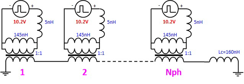
Consider aggressive loading transient in a 12V to 1.8V application, where all high-side FETs in all phases turn on as fast as possible, so the (VIN - VO) = 10.2V voltage is simultaneously applied to all main windings as shown in Fig.2. In the worst case, all 1:1 transformers would generate 10.2V on their secondaries so the resulting voltage pulse on the secondary side would be (VIN - Vo) ×NPH. This is clearly a concern for safety. Fig. 2 has some typical ballpark values for the TLVR, the small leakage between the main and auxiliary windings was measured as 5nH.
Click image to enlarge
Figure 2: An equivalent schematic of TLVR = 150nH with a worst-case loading transient
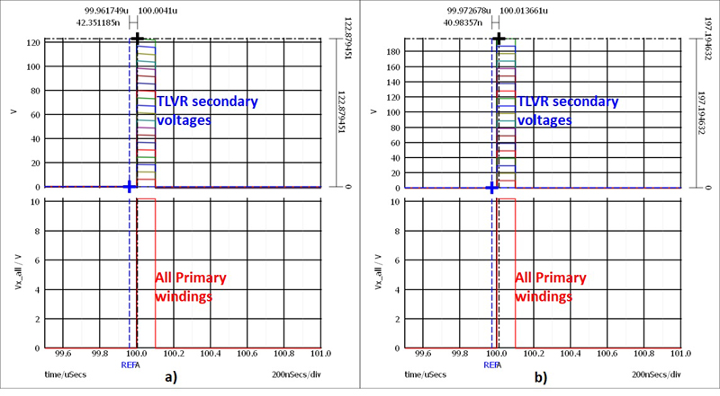
Fig. 3 shows simulations for NPH = 20 when all VX switching nodes have a 100ns pulse of 10.2V. All secondary TLVR voltages are plotted to show how a series connection of the windings builds up the voltages. When the secondary windings of 20 linked phases are loaded with LC = 160nH a) – the voltages on the board reach ~123V. But if LC is disconnected b), the voltage step can be as high as 197V. The total voltage is closer to the worst case (VIN - Vo) ×NPH.
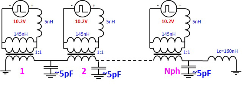
However, the results in Fig. 3 are still too optimistic. In reality, the simplified simulation in Fig. 3 needs to add at least parasitics capacitances between the GND plane and fairly wide traces that connect secondary TLVR windings, on the order of 5pF. Related schematic in Fig. 4 leads to the simulations shown in Fig. 5. Capacitors result in a lot of oscillations in the high-Q circuit. The same NPH = 20 case shows a voltage peak of 239V when LC = 160nH is present, and 390V, if LC is broken off the board.
Notice that the value of the parasitic layout capacitors does not really matter – it only affects the frequency and envelope of oscillations, but not the amplitude.
Click image to enlarge
Figure 3: TLVR worst-case transient simulation with a) LC = 160nH, b) LC is open, NPH = 20
Click image to enlarge
Figure 4: Layout capacitances are added to the TLVR equivalent transient schematic
Click image to enlarge
Figure 5: TLVR worst-case transient simulation with 5pF per secondary node added, a) LC = 160nH, b) LC is open, NPH=20
One approach to mitigate this is to make sure that phases cannot align during the transient, but it would clearly put a limit on the transient response. Another approach is to limit the number of linked TLVR phases. But what are the practical limits of this approach, as NPH needs to be high enough for current ripple impact to be small for efficiency, while NPH also needs to be low enough to limit worst-case secondary voltage?
Considerations for Linked Nph
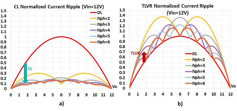
Fig. 6 compares normalized current ripple for a coupled inductor and for TLVR as a function of Vo (for VIN = 12V). Starting with a discrete inductor L (red curve), different number of Nph are either a) magnetically coupled as a single coupled inductor or b) electrically linked as TLVR. Assumptions used: TLVR = 150nH with leakage 5nH, LC = 120nH. Coupling ratio LM/LK = 5 is assumed for CL. Depending on NPH, the magnetically coupled inductor significantly reduces current ripple from a discrete inductor with the same value L. The TLVR current ripple, on the other hand, is always larger than in a discrete inductor with the same value L. The TLVR current ripple also has notches at the D = k/NPH areas. Increasing the number of linked phases is clearly beneficial in decreasing the TLVR current ripple (Fig. 6b).
Click image to enlarge
Figure 6: Calculated normalized current ripple for different NPH as a function of Vo (VIN = 12V) in a) coupled inductor (LM/LK = 5) and b) TLVR = 150nH (LC = 120nH)
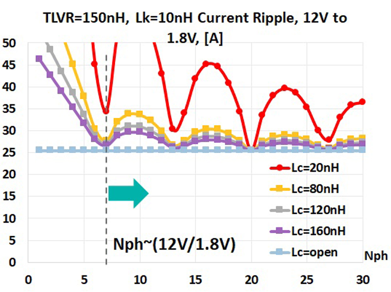
Fig. 7 shows current ripple as a function of linked NPH for TLVR = 150nH and different values of LC. Lower LC values introduce larger error, but the trends are very clear: lowering NPH or decreasing LC leads to an increase in current ripple. Notice that TLVR always has a larger ripple than a “baseline discrete inductor” (LC = open). It can be concluded that the minimum number of linked phases should be around NPH_min~1/D, to keep the current ripple impact under control. In other words, increase NPH at least up to the first notch in the current ripple curve where duty cycles of different phases get close to overlapping.
Click image to enlarge
Figure 7: Calculated current ripple in TLVR = 150nH for different LC as a function of linked NPH (VIN = 12V, Vo = 1.8V, fS = 400kHz)
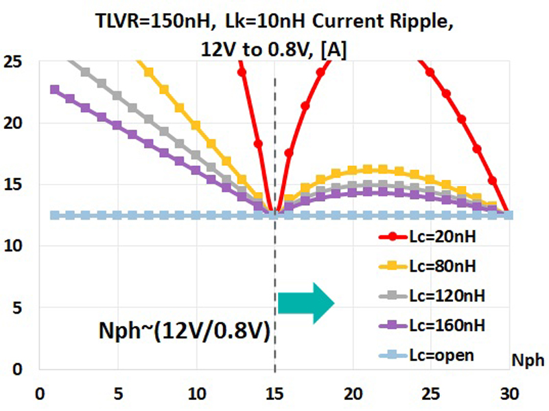
Another conclusion is that the minimum desirable number of linked phases will increase with lower Vo as in (1).For VIN = 12V and Vo = 1.8V, the TLVR solution roughly needs NPH_min~6, while for Vo = 0.8V it would be NPH_min~15, see Fig.8. Of course, a smaller number of NPH is acceptable if some extra impact on current ripple and therefore efficiency is tolerated.
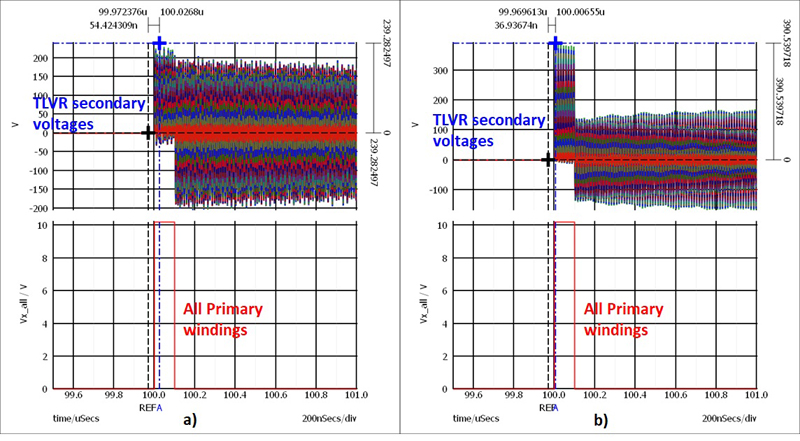
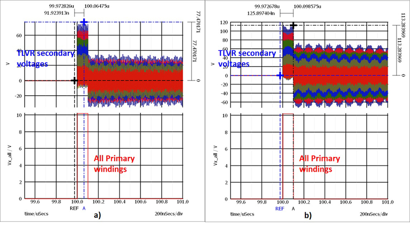
Assuming 12V to 1.8V applications, linking NPH = 6 is targeted to keep the TLVR current ripple down. Fig.9 shows the secondary TLVR voltage when all phases on primary have a 100ns pulse (VIN - Vo). When LC = 120nH is present, the voltage on the secondary can reach 77V. If LC is broken off the PCB, the unloaded secondary voltage can oscillate up to 113V.
Click image to enlarge
Figure 8: Calculated current ripple in TLVR = 150nH for different LC as a function of linked NPH. VIN = 12V, Vo = 0.8V, fs = 400kHz
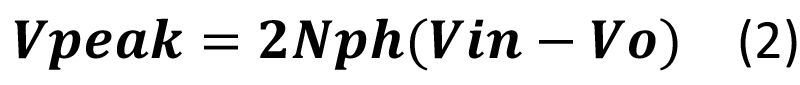
A rough estimate for the worst-case secondary TLVR voltage would be as shown in (2), where the 2x multiplier is coming from the oscillation instead of a pulse waveform.
Correspondingly, the estimated VPEAK would be 408V for NPH = 20 and 122V for NPH = 6, compared to the simulated 377V (Fig. 5b) and 113V (Fig. 8b), respectively.
Click image to enlarge
Figure 9: TLVR worst-case transient simulation with 5pF per secondary node added, a) LC = 120nH b) LC is open, NPH = 6
Then the estimated NPH_max to keep the worst-case secondary voltage under the desired minimum VPEAK could roughly be as shown as (3). Assuming a 60V maximum voltage rating, a 12V to 1.8V application would have NPH_max < 2.9 and for a 12V to 0.8V application, NPH_max < 2.6. This creates a problem with keeping the current ripple contained, because of NPH_min = 6 and NPH_min = 15 for Vo = 1.8V and Vo = 0.8V, respectively. If a safety rating requires a low enough voltage limit, then it seems that in practical applications, an extra current ripple increase would occur and therefore a more noticeable efficiency impact is expected.
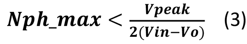
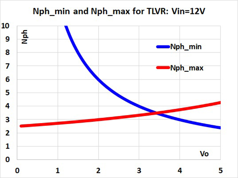
Fig. 10 shows NPH_min (efficiency) and NPH_max (safety) as a function of Vo, assuming a safety rating of VPEAK = 60V and VIN = 12V. A possible solution between NPH_min and NPH_max exists only above Vo = 3.5V, but NPH_max overrides it at lower voltages due to safety concerns, which leads to higher current ripple and related efficiency impact.
Click image to enlarge
Figure 10: NPH_min (efficiency) and NPH_max (safety) as a function of Vo, assuming VIN = 12V and a safety rating of VPEAK = 60V
Of course, if NPH is lowered, this also leads to an increase of the total number of added tuning inductors, LC, since each linked group needs one.
Conclusion
The TLVR approach is an improvement from a discrete inductor, but it mainly improves the transient while making a current ripple and therefore makes efficiency worse. To keep current ripple impact under control, linking NPH_min > VIN/Vo could be recommended. From the safety perspective, if the VPEAK limit for the worst-case voltage on the PCB is desired, then linking no more than NPH_max < VPEAK/((VIN - Vo) ×2) phases is needed. Safety standards would generally override the current ripple considerations, so a hit in current ripple impact and efficiency in the TLVR approach is to be expected.
The other possibility to mitigate high voltage concerns is to ensure that the controller never aligns more than some maximum number of phases, according to NPH_max described above (2 to 3 phases max for 60V limit, etc.) The challenge with this approach is that it would limit how fast the system transient performance can be. Overlapping too many phases in steady-state operation should also be considered.


