Click image to enlarge
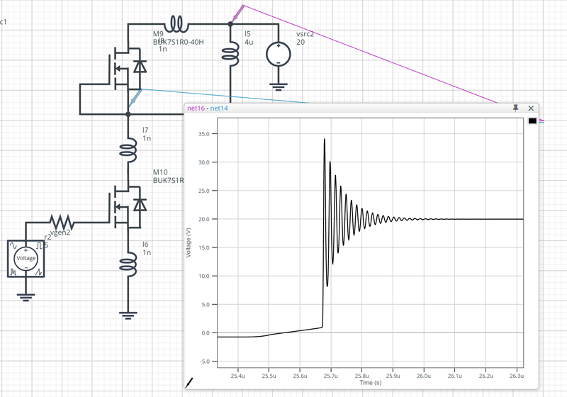
Figure 1: Double pulse testing using standard power MOSFET models
One of the biggest challenges facing engineers when designing with discrete power MOSFETs is the fact standard simulation models provided by many manufacturers are limited in how well they emulate real-world performance. This reduces the usefulness of SPICE simulations when attempting to understand how a circuit will perform in a practical application. For example, most standard models can only be used to simulate how a discrete device will behave at a nominal temperature (typically 25°C). Standard simulation models are usually not comprehensive because they neglect to include some important device parameters that could provide some insight into the electromagnetic compatibility (EMC) performance of a circuit, for example. In this regard, discrete circuit designers could be considered the “poor relation” of their integrated circuit design counterparts who are spoiled by all-encompassing models that leave nothing to chance.
In this article we explore the limitations of standard models for power MOSFETs in more detail by simulating a simple half-bridge circuit typically used in a range of motor control applications. We then simulate the same design using a new and much more advanced set of electrothermal models which have been developed to provide circuit designers with much greater and more accurate insight into how their devices will really perform in on a printed circuit board (PCB) in a real-world application.
Limitations of standard models
In order to correctly predict the switching and EMC behaviour of a MOSFET, it is critical to have an exact model of its static and dynamic characteristics across the full operating temperature range. This allows accurate circuit simulations to be performed using a SPICE software package. Standard models provided by many device manufacturers cannot be fully relied upon because they do not provide all of this information, meaning discrete designers are sometimes required to make assumptions about aspects of device behaviour and must therefore err on the side of caution by assuming worst case scenarios will occur. Adopting this approach can mask more subtle board-level performance issues or even result in designs which are over-specified for their purpose. In most cases, the available models cannot be used to gain any insight into the EMC performance of a device before a board is physically constructed.
Power MOSFET testing
Double pulse testing is an industry standard method used to characterize the switching behavior of power semiconductors specifically intended for testing device performance in inductive clamp switching applications. It consists of a half-bridge configuration with an inductive load with a low-side MOSFET switch and a high-side MOSFET configured to act as a freewheeling diode (Figure 1). A train of two pulses is applied to the gate of the low side MOSFET (hence the test name). The first pulse turns on the low-side MOSFET causing current to flow through and charge up the inductor. Next, the gate signal is grounded, and this turns off the MOSFET causing the current in the inductor to begin flowing through the body diode of the high-side freewheeling MOSFET. During this time charge accumulates in the P-N junction of the high side body diode - this is referred as reverse recovery charge (Qrr). Once the second pulse is applied to the gate of the low-side device, it switches on again. This causes current to once again flow in the circuit, but the charge previously stored in the P-N junction of the upper device must also be removed. This Qrr charge creates a short-duration, high-frequency transient signal (referred to as reverse recovery current) which interacts with the parasitics on the PCB and in the MOSFET itself. This phenomenon affects the EMC performance of the circuit because of the voltage and current overshoots which result. To accurately determine the magnitude of this effect, it is important for device models to capture the reverse recovery behavior of the body diode so that the frequency and damping of the resulting oscillations (ringing) can be measured. This reverse recovery diode behavior is not normally captured in the simulation models provided by many manufacturers and as a result, the magnitude of the ringing caused at second switch-on can appear to be quite large. For example, Figure 1 shows the results of a double-pulse simulation using a set of standard MOSFET models showing a 75% voltage overshoot that lasts for almost 0.5 microseconds. When real devices are subsequently evaluated in the lab, this amount of ringing does not occur in practice. The discrepancy is caused by the fact that the standard model does not capture the reverse recovery behaviour of the body diode. This is a concern because the amount of ringing is sufficient to hide other effects that may occur due to the presence of other parasitic effects, and these may only be revealed to be problematic once a board has been constructed. The limitations of these models mean they cannot be used to gauge the EMC performance of the circuit and it can only be quantified after extensive lab testing is performed much later in the product development process. At this stage, any design changes that might be required to help improve EMC performance become much more difficult and costly to implement.
Advanced electrothermal models
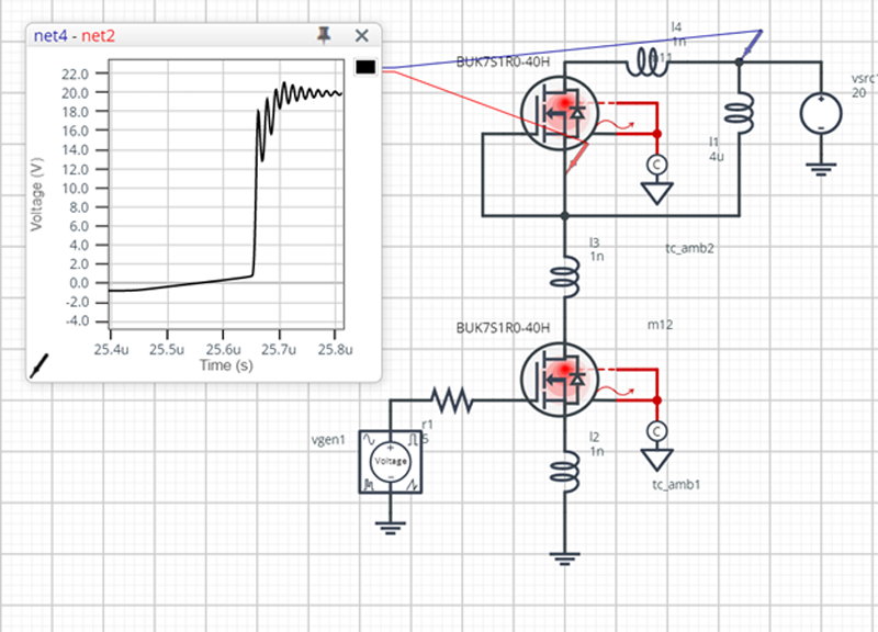
Nexperia recognized the limitations of standard MOSFET models and set about developing a new set of advanced electrothermal models for use with SPICE and VHDL-AMS that more accurately captured the behaviour of their power MOSFET devices. These now also include an accurate model of reverse recovery for the body diode. For example, Figure 2 shows the results of the same device simulation (a BUK7S1R0-40H N-channel 40 V,1mΩ MOSFET in LFPAK88) performed previously, but which uses these advanced models. Much less ringing is evident, and oscillations settle out in a much shorter time interval (less than 0.2 microseconds) than was the case using standard models.
Click image to enlarge
Figure 2: Double pulse testing using advanced electrothermal power MOSFET models
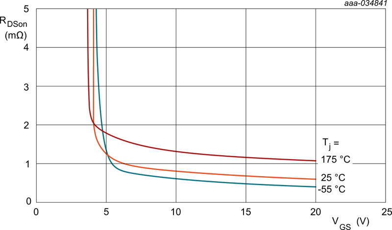
These models reflect much more accurately the actual performance measured in the lab with the discrepancy between simulated and lab measurements being as low as 0.9% for some parameters. This increased accuracy allows designers to be much more confident in gauging what the real-life EMC performance of their circuit will be. Apart from more accurately capturing device behaviour, these models can also be used to examine device performance across the full operating temperature range. Figure 3 shows the simulated on-resistance (RDS-ON) for the same MOSFETs at temperatures ranging from -55°C and 175°C, but simulations can be also performed at any desired temperature. This provides designers with the ability to understand more how their application will perform at operating temperature ranges expected for different applications.
Click image to enlarge
Figure 3: RDSON of Nexperia BUK7S1R0-40H Power MOSFET across the full temperature range of operation
Conclusion
Standard power MOSFET simulation models provided by many manufacturers fail to include some vital device parameters which are required to provide insight into circuit performance characteristics like EMC. These can also usually only be used to simulate how a device will perform at a nominal temperature. These limitations often result in designs being unnecessarily over-specified or problems going undetected until late in the product development process, when they become difficult and expensive to address. A new set of advanced electrothermal models by Nexperia accurately model the reverse recovery of the body diode in their power MOSFETs and also allow designers to simulate device behaviour across the full operating temperature range. These features represent a significant advance on standard models, allowing designers to be more confident in the results of their SPICE simulations and to gain insight into the EMC performance of their circuit at a much earlier stage in the development process.
 PDF
PDF