Toshiba expands family of ultra-mini load switches
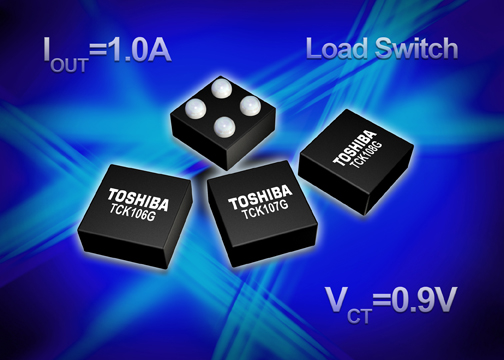
Toshiba Electronics Europe has expanded its family of ultra-miniature, low-power CMOS load switch ICs. The TCK106G, TCK107G and TCK108G belong to the family of 1A switches that help to reduce the board space needed for power management circuitry in mobile phones, tablet PCs and other high component density portable applications. Each of the new switches is supplied in a 4pin Wafer Level Chip Scale Package (WCSP4) with maximum dimensions of just 0.79mm x 0.79mm. Despite the compact size, the new switch ICs offer integrated features such as a slew rate control driver circuit together with a wide operating voltage range. As a result, the ICs reduce the component count and thus the board space requirements when compared to designs based on discrete MOSFETs. The switches operate with an input voltage range from 1.1V to 5.5V and a minimum control voltage of VCT=0.9V. They offer very low loss performance at 500mA load current with the typical ON resistance values between 49 and 83mW for input voltages of 5V and 1.8V, respectively. Additionally, intrinsic losses are kept to a minimum with quiescent and standby currents of 80 and 50nA, respectively. The OFF state leakage current is in the range of 14nA within the operating temperature range of -40 to 85°C. All of the new load switches incorporate an integrated slew rate control driver to minimise the risk of damage due to inrush current transients. The TCK107G and TCK108G also have an auto-discharge function for enhanced load control. Furthermore, it is possible to select between an �active low' (TCK108G) and �active high' (TCK106/107G) version, where the TCK106G and TCK107G utilize an integrated pull-down resistor to guarantee defined IC operation even if the control terminal is left open. Toshiba