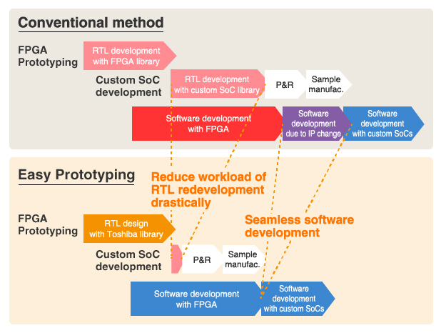
Toshiba Corporation announced the immediate availability of “Easy Prototyping”, a solution that allows reuse of the design assets required to develop large scale custom SoC with FPGA prototyping. Adoption of the solution dramatically shortens the development time from FPGA prototyping to custom SoC development. Easy Prototyping is available on Toshiba’s ASIC and FFSA platforms.
In conventional FPGA prototyping, SoC designers cannot reuse FPGA hardware and software design assets for custom SoC development because FPGA libraries and IPs are FPGA specific. Easy Prototyping facilitates the reuse of these assets for custom SoC design by adapting the FPGA prototyping libraries, leveraging Toshiba’s libraries and IP subsystems. This enables designers to identify the interface and easily switch between FPGA prototyping and SoC implementation with the Toshiba provided wrapper logic.
Toshiba supports third party IP with a good track record in FPGA and provides them as subsystems that are verified for connectivity with Toshiba’s custom SoC solutions. 10 Gigabit Ethernet (MorethanIP), PCI Express 3.0/2.1/1.1 (Northwest Logic), DDR3 SDRAM controller (Northwest Logic) are available immediately for Easy Prototyping, and the line-up is being expanded to cover additional solutions.
Going forward, Toshiba will continue to provide solutions that help customers to optimize system design and achieve timely product development.