Transient Protection Solutions in Automobiles
ESD-Safe MLCCs, Slow Transient Wave-Rated MLCCs, and Multilayer Varistors
Thanks to modern technology, passenger vehicles are now safer, more enjoyable, and more efficient than ever. Today’s automobiles utilize incredible amounts of computing power to improve the overall driving experience in several different ways. For example, arrays of sensors and dedicated processing units now monitor and make use of vast amount of data from systems spanning cabin entertainment electronics to critical underhood modules. Multiple central processing units now employ high-speed networks to transmit data to even larger and more powerful processors that profile, prioritize, and control numerous sub systems. In addition, automobiles now utilize RF links to communicate with both one another and surrounding infrastructure.
The complexity of automotive ICs and the often critical nature of their high-reliability performance helps support the argument that these increasingly prolific devices are now more susceptible than ever to transient voltages. Automotive design engineers generally use shielding and routing methods to redirect transients, transient voltage suppressors to clamp the effects of incoming transients, or integration capacitors to capture transient voltages and slowly release their energy back into the circuit at levels below the susceptibility limit. However, due to the varying nature of these device’s cost, size, and performance limitations, there is no “one size fits all” solution for each and every automotive application.
This article examines two automotive transient voltage control options, transient voltage suppression clamps (i.e., multilayer varistors) and integration capacitors, and compares and contrasts multilayer varistors, ESD-Safe MLCCs, and slow-pulse capable multilayer ceramic capacitors.
Performance Considerations
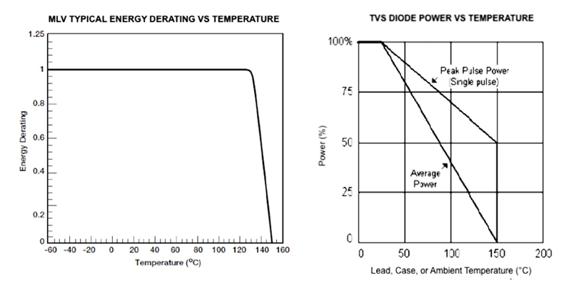
The ideal method of transient voltage suppression is to clamp the transient voltage with a transient voltage suppressor (TVS). Of all the TVS devices available on the market, multilayer varistors (MLVs) are one of the best choices due to the fact that they are small, lightweight, and capable of both clamping voltages in their on-state and acting as an electromagnetic interference (EMI) filter in their off-state. Additionally, MLVs do not have the same severe power derating limitations as TVS diodes do (Figure 1). This feature is increasingly important in automotive LED drivers and engine electronics, as these applications are frequently subjected to operating temperatures approaching or even exceeding 125°C.
In some cases, ICs have a level of on-chip protection or are located deeply within the inner portion of a PCB or module. In these instances, an integration capacitor can often be used to attenuate the front-end, rise-time effects of the transient. This type of protection, electrostatic discharge (ESD) integration, is best suited for non-critical automotive applications. In instances where communication bus structures need transient control, MLVs are a more effective transient voltage solution, as the magnitude of capacitance needed within an integration capacitor would cause signal data skew.
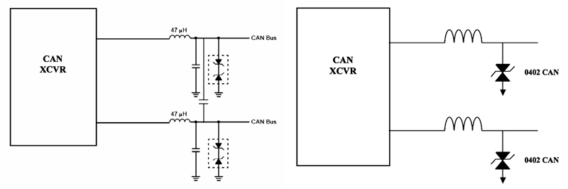
Modern vehicles have several dozen CAN interfaces that require transient voltage control. Figure 2 illustrates a typical CAN circuit both before and after the implementation of CAN MLVs. In this example, an MLV is connected from both the CANH and CANL lines to the ground and is used to provide EMI filtering in the varistor’s off-state and to provide bidirectional protection for the IC when ESD or other transients are present, making it an effective replacement for both the EMC capacitor and the bidirectional diodes used in the circuit with a single MLV. MLVs are also well suited for use in automotive CAN circuits due to the fact that several series can operate at 150°C without the need for derating. So, as CAN interfaces and other communication buses continue to expand their roles to underhood applications, the case for the use of MLVs will only become stronger.
Click image to enlarge
Figure 2: A typical CAN circuit with two MLCCs and two diodes (left) and a typical CAN circuit with either two MLVs or one two-element MLV array (right)
In circuits that utilize ICs with on-chip protection or ICs integrated within a PCB or module, or in applications where automotive circuits employ lower cost, slower, and less complicated ICs, the ICs will exhibit at least a moderate degree of inherent ESD survivability. So, ESD integration capacitors can provide effective transient voltage protection in these types of circuits. However, it is important to understand that these solutions are only effective in the case of short-waveform incidents upon fairly rugged ICs in non-critical applications that can withstand large amounts of capacitive loading. Luckily, though, that combination of qualities is fairly common. In most engine control units (ECUs), there is typically an 80/20 need for ESD integration capacitors versus MLVs on the pins. For example, a 300-pin ECU would have a 240:60 ratio of integration capacitors to MLVs.
ESD Models
ESD is a sub-nanosecond rise-time event that is generated by the charge transfer of materials in the tribo-electric material series. ESD can be either positive or negative in polarity, contact- or air-discharge, and repetitive or random in nature.
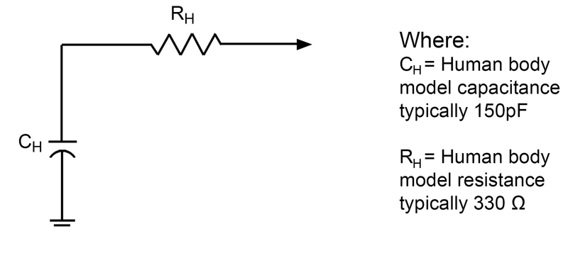
An ESD event is typically modeled by a capacitor charged to a particular voltage level in series with a current-limiting resistor, both of which are discharged at particular repetition rates to simulate a certain number of real-world transients on the device under test (DUT). There are several models that can be used to simulate the various transient sources that could inject ESD into a victim, but the three most common are the charged device model (CDM), the machine model (MM), and the human-body model (HBM).
ESD-Safe MLCCs are generally intended for use in IEC 61000-4-2 applications subjected to HBM strikes (150pF, 330Ω), but not exclusively in contact discharge mode (Figure 3). Although there are many common transients that are slow in speed, ESD-SafeMLCCs are primarily intended for use in fast transients hardening.
Click image to enlarge
Figure 3: The human-body model (HBM) is one of the three most common models that can be used to simulate transient sources that could inject ESD into a victim.
Transient Voltage Control via Multilayer Varistor (MLV) Clamping
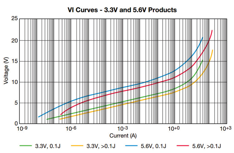
Multilayer varistors are zinc oxide (ZnO2) ceramic semiconductors that exhibit nonlinear voltage-current (VI) characteristics in the presence of an electric bias. The number of grains between the multilayer conducting electrodes determines the breakdown voltage, which is defined as the 1mA current conduction point on the VI curve. Clamping voltage is defined as the maximum voltage measured with an 8x20µs waveform applied at a specific current magnitude defined by the energy rating of the part. Another parameter of MLVs is operating voltage, which is the steady-state voltage that can be indefinitely applied to the MLV without causing an increase in the specified leakage current of the part.
Figure 4 shows the VI curve for an MLV acting as a TVS clamp. MLVs offer advantages over other TVS clamps, such as diodes, and significant advantages over MLCCs, including large in-rush current capabilities, high-energy transient voltage suppression, off-state bulk EMC capacitance, an extremely low failure-in-time (FIT) rate, and ease of assembly. These benefits make MLVs attractive solutions for circuit protection in advanced automotive systems.
Click image to enlarge
Figure 4: MLV voltage-current (VI) curves
Transient Voltage Control via MLCC Integration
Many transient voltage control designs utilize a capacitor at the I/O pin to integrate the voltage and protect the IC from ESD damage. Although this can be an effective design practice, engineers often overestimate the capacitor's performance due to its significant value drop upon the applied ESD event.
Generally speaking, the amount of capacitance drop for NP0 dielectrics is negligible. However, the amount of capacitance drop for X7R capacitors can be 50% or greater. This value also varies from manufacturer to manufacturer and on a lot-by-lot basis within any particular manufacturer, as ESD voltage coefficient is not characterized on a lot-by-lot basis for standard capacitors.
The capacitance drop from the expected value of a standard X7R capacitor can result in a much higher voltage at the IC or device that needs to be protected. ESD capacitors can be an effective weapon in the control of ESD events, but designers should exercise extreme care during the device selection process.
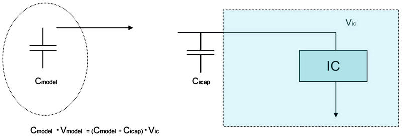
The conservation of charge applies to the capacitance voltage product of the ESD model and the combined capacitance of the ESD model plus the ESD integration capacitor (Figure 5). This can be represented by the equation Cmodel x Vmodel = (Cmodel + Cicap) x Vic, in which Cmodel is the capacitance of the ESD model, Vmodel is the voltage to which the model is charged, Cicap is the capacitance value of the integration capacitor, and Vic is the voltage that the IC (or device to be protected) experiences.
Click image to enlarge
Figure 5: The conservation of charge applies to the capacitance voltage product of the ESD model and the combined capacitance of the ESD model plus the ESD integration capacitor.
The original charge of the ESD model is split between the ESD model's capacitance and the ESD integration capacitor. For example, if the capacitor in the ESD model is rated for 150pF and charged to 8kV, and the integration capacitor is rated for 1,000pF, the expected surge voltage at the IC would be approximately 1,044V.
ESD Capacitor vs. MLV HBM ESD Testing
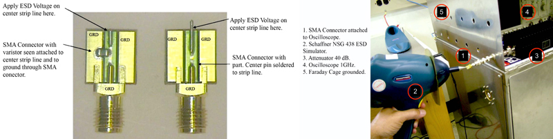
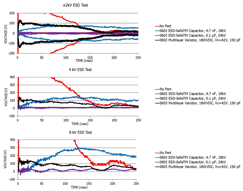
Human-body model (HBM) ESD tests were performed on two common MLCCs and an MLV in an effort to determine the effect of each device on an ESD waveform of varying magnitude in an IEC 61000-4-2 application. In this test, the DUT was soldered to a test card terminated with an SMA connector that connected to an entry port on a faraday-shielded 40dB attenuator that connected to a TDS 784 oscilloscope. Test set-up and definition is shown in Figures 6.
Click image to enlarge
Figure 6: An optimized ESD component test fixture (left) and equipment set-up
The test proceeded with the contact discharge of positive and negative transients of 2kV, 4kV, and 8kV ESD strikes to the DUT. The resulting voltages captured are representative of the ESD voltage magnitude at the port of the device to be protected. The graphs pictured in Figure 7 illustrate the relative protection of a 4.7nF X7R dielectric MLCC, a 100nF X7R dielectric MLCC, and an 18V MLV, and the difference between integration and clamping devices.
Click image to enlarge
Figure 7: The relative protection against positive and negative 2kV transients (top), 4kV transients (middle), and 8kV transients (bottom) that a 4.7nF X7R dielectric MLCC, a 100nF X7R dielectric MLCC, and an 18V MLV provided the DUT.
The 2kV graph shows the effect of positive and negative waveforms on all three of these devices. Since both the MLCCs and MLV are non-polar, the graph is symmetrical. The integrated voltage of the MLCC increases as the transient voltage increases, while the MLV exhibits a relatively constant clamping voltage regardless of the ESD transient magnitude.
These tests illustrate that larger-value capacitors will integrate the transient voltage to a lower voltage level. However, as mentioned, there is a practical limit to the amount of capacitance loading that a circuit may allow. Voltage lines have virtually no capacitance limit, while signal and data lines have a concrete value of integration capacitance they can handle before experiencing signal degradation.
The following table depicts the range of commonly available ESD capacitor and MLV sizes.

Click image to enlarge
Figure 8: Technical specifications for ESD-Safe MLCCs and MLVs
Slow Transient Waveform MLCCs
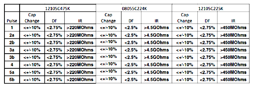
There are also MLCCs especially designed to survive slow transient waveform injections. These devices are designed and tested to suppress transients including ISO 7637 pulses 1, 2A/B, 3A/B, 4, and 5A/B, along with GS95003-2 load-dump transients. State-of-the-art, slow-wave MLCCs are available in 0603 to 1210 case sizes, capacitance ranges spanning 1nf to 4.7µf, and with dissipation factor (DF) and insulation resistance (IR) values as shown in Figure 9.
Click image to enlarge
Figure 9: Dissipation factor (DF) and insulation resistance (IR) values for low transient waveform pulse MLCCs
Summary
Today’s automotive design engineers have a wide range of transient voltage control solutions to choose from and can match various solutions to individual application demands. MLVs exhibit significant electrical, physical, and reliability advantages over TVS diodes and integration capacitors, and testing has shown that ESD-Safe MLCCs can be used to effectively control ESD transient waveforms in certain applications as well. Newer solutions include slow transient wave MLCCs, which have been proven to survive ISO pulses.
AVX