Author:
Isaac Sibson, Automotive Applications Engineer, Diodes Incorporated
Date
07/22/2019
 PDF
PDF
Click image to enlarge
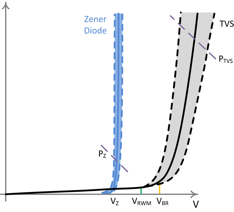
Figure 1: A TVS is designed to operate differently to a Zener diode, and for a shorter period
Anyone who has worked with integrated electronic devices in a design, production or repair environment will be familiar with the anti-static or electrostatic discharge (ESD) wrist strap, and knows their purpose is to protect ICs before they are inserted into or onto a PCB. Manufacturers fully understand the damage electrostatic discharge (ESD) can cause, both during and after production. Similarly, the persistent threat present from transient voltages, generated by natural phenomena such as lighting strikes, as well as artificially by the electrical operating environment is particularly apparent in harsh environments such as industrial and automotive. A single transient could easily damage or disrupt a sensitive electronic component, while noise (unwanted signals) of even modest energy can cause significant interruption to digital communication transmissions.
Transients can occur as momentary or continuous surges wherever high voltages are present, and can propagate unchallenged through PCB tracks and cables. Momentary surges can easily reach 3kV and can often occur when inductive loads are switched – due to something as simple as a relay being operated or a motor started or stopped. As the majority of modern ICs operate from low DC voltages, transients are a common threat to integrated circuits and digital signals, present in applications across all sectors.
Combating the Voltage Surge
The transient voltage suppressor (TVS) is a solid-state device, designed to provide a low-impedance path to a transient voltage but a high-impedance path at all other times. This allows supply voltages and signals to operate as intended, but almost instantly clamps any high voltages safely, protecting sensitive components.
A TVS is effectively a PN junction diode designed to enter avalanche mode when the potential on the cathode exceeds a predetermined level. The level chosen will depend on the application, but the crucial characteristic is that the junction breaks down as quickly as possible, in less than one nanosecond. It would normally be placed either in parallel with the load across the 0V and supply rail, between ground and a single-ended signal, or across a differential pair of signals.
While it may resemble the Zener diode, a TVS is designed to operate slightly differently. A Zener diode is designed to repeatedly and continuously operate in breakdown mode at an accurately defined voltage, providing a stable reference or working as a limiter. It would be expected to operate in this mode all the time the voltage present is greater than the upper voltage limit and be able to withstand a modest continuous current passing through it. A TVS, on the other hand, is not designed to conduct for any length of time; instead it is designed to break down quickly and absorb a higher amount of energy for a shorter time, which is commensurate with the profile of a surge or transient voltage.
While a Zener diode would normally be specified at a specific voltage level, a TVS would be specified based on the nominal working voltage. This means, for example, that to protect a microcontroller operating at 3.3V, a TVS of 3.3V could be used. The actual parameter being specified in this case is the reverse working voltage (VRWM), defined as the voltage at which the device is guaranteed not to pass more than a minimal specified leakage current (e.g. less than 10µA). In other words, VRWM is the voltage at which the TVS has a negligible influence on the rest of the circuit.
The related breakdown voltage parameter (VBR is the point where the device will conduct at least a specified minimum current (e.g. 10mA).
The key understanding is this:
VRWM is guaranteed to conduct less than IR (e.g. 1-10µA)
VBR is measured at IT (e.g. 10mA)
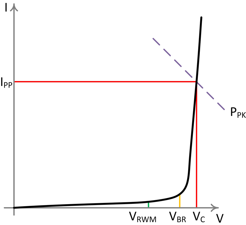
As shown by the dotted lines in Figure 1, VBR can have a tolerance so it is important to consider this variation with respect to the circuit being protected. The device’s Peak Pulse Power limit, or PPK, can be found on the transfer characteristic of a TVS, as shown in Figure 2. The point at which the transfer curve intersects PPK denotes the maximum clamping voltage (VC) and maximum peak current (IPP) for the device.
Click image to enlarge
Figure 2: The transfer characteristics of a typical TVS
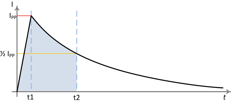
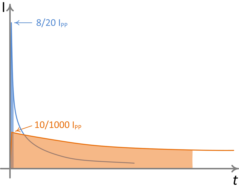
The length of the pulse is an important consideration as this dictates the amount of energy to be absorbed. Standard duration and magnitude pulses are defined in international standards, including IEC 61000 and IEC 61643. The former covers fast surges such as those caused by ESD discharges and lightning strikes, and defines two relevant points on the power curve: 8µs (t1) and 20µs (t2) – these are commonly referred to as 8/20. The latter standard deals with slower surges with higher energy levels, such as those that would occur from inductive loads. The time intervals for this standard are 10/1000, which equals 10µs (t1) and 1000µs (t2). These figures are used to define TVS performance, as shown in Figure 3. Note that t2 is total elapsed time from 0.
Click image to enlarge
Figure 3a & 3b: Figure 3a shows how the points t1 and t2 are used to define the energy in the spike, while figure 3b shows the shape of the surges defined by the IEC standards. The shaded areas represent the energy of the pulses
TVS for Automotive
The main voltage rail system in most cars is 12V DC generated by the rectified output of an alternator, which is inductive and therefore also a potential source of transient voltages. As the features in cars become more automated they include an increasing number of smaller motors, for powering features such as mirrors, windows and seats. In addition, the electrification of the drivetrain results in mechanical systems such as water and oil pumps being driven by electric motors. All of these represent an inductive load on the system, becoming a potential source of transient voltages.
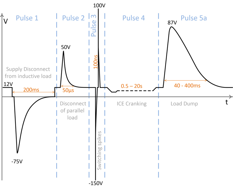
Understandably, there are additional standards to cover surge protection for the automotive environment, including ISO 7637-2 and ISO 16750. Figure 4 shows the shape of the test pulses defined by these standards.
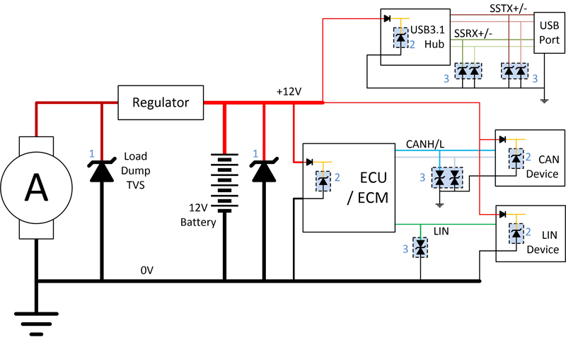
The circuitry must demonstrate that it is capable of dealing with each of the pulses shown in Figure 4 (the pulses are not shown to scale). Designing to meet these requirements may involve using several TVS devices distributed around the entire system. For example, there will likely be a main load-dump TVS located close to the alternator, which would be physically large and chosen based on the characteristics of the system (Figure 5). The remaining energy would need to be dissipated by supplementary TVS protection within each module, and a system-level approach should be used to define the requirements for this.
Click image to enlarge
Figure 4: A representation of the test pulses used in the automotive industry
Click image to enlarge
Figure 5: A depiction of where TVS devices are used in an automotive application. Large devices around alternator and regulator; TVS and reverse polarity protection around electronic modules and protection around data buses
In harsh environments there will be a significantly larger area under the curve of the pulse, corresponding to more energy to be dissipated. This is more apparent in automotive applications and the specifications reflect this, particularly when contrasted with the spikes defined in the standards mentioned earlier.
Protecting safety-critical signals with TVS devices
As modern vehicles make greater use of inter-module communications, the use of automotive-qualified TVS devices for signals such as CAN, FlexRay and LIN is increasing. These buses are used to carry safety-critical communications between automotive modules; signals that may be interrupted by lower energy noise. The need here is to protect the signals and the modules without impacting the signal bandwidth. As CAN and FlexRay are differential buses, they require a dual bidirectional TVS to protect both lines.
A bidirectional TVS is designed to provide protection from transients across a split-rail system or differential signaling scheme, to protect from transients that are both positive and negative with respect to the signal. These devices are designed to be either symmetrical or asymmetrical; the former offers the same breakdown voltage level in both directions, while the latter features a reverse breakdown voltage that is higher in one direction than the other.
The LIN bus would employ an asymmetrical bidirectional TVS, for example, because the signal line can easily fluctuate between -15V and +24V due to ground variance.
Conclusion
Transient voltages are an ever-present threat to sensitive integrated circuits, and in some application areas (such as automotive), they are an unavoidable hazard. Meeting the challenge of providing protection against surges, spikes and transients is the job of the TVS.
The choice of a TVS solution is highly system dependent as designs vary considerably even for the same end product. A supplier such as Diodes Incorporated, which offers a wide range of TVS protection for vertical sectors, including consumer, industrial and automotive, works closely with designers to fully understand their system requirements and recommend customized TVS solutions for them. In this way, every part of the electronic system can be protected from hazardous transients, delivering greater reliability and safety.
Diodes Incorporated