Author:
Siddarth Sundaresan, Sr. VP of Technology, Sumit Jadav, Sr. Director of Technical Marketing (GaN & SiC), Arash Salemi, Senior Manager Technical Marketing and Jaehoon Park, Director of SiC Device Technology, all Navitas Semiconductor
Date
10/20/2025
 PDF
PDF
Click image to enlarge
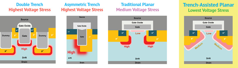
Figure 1: Cross-sectional views illustrating the cell pitch for different Power MOSFET technologies: double trench, asymmetric trench, traditional planar, and trench-assisted planar technologies
The two established architectures of silicon carbide (SiC) MOSFETs for high-power systems – planar and trench – both present a fundamental unappealing compromise for power engineers.
The manufacturing simplicity of the planar gate structure enables increased yields and therefore lower costs. This structure is also more robust than the trench gate and so offers the engineer improved reliability/MTTFs.
However, this comes at the cost of a higher specific on-resistance (RON,SP) and with this comes poorer current density and conduction losses.
Conversely, by creating a vertical channel, the trench gate architecture offers a lower RON,SP and higher power density. But it relies on a more complex and costly manufacturing procedure, requiring about 40% more process steps than planar and having a lower yield. Additionally, the technology’s high electric field concentration at trench corners can stress the gate oxide and therefore poses a long-term reliability risk.
For many applications, these two extremes make for a poor compromise and force the selection to be a least-worst option.
This article examines a novel trench-assisted planar architecture that resolves this fundamental conflict by combining the strengths of each approach. The result is a better middle ground with a significantly improved RON,SP versus planar architectures but without sacrificing affordability and reliability.
The Trench-Assisted Planar Architecture
Navitas’s trench-assisted planar technology sits within the company’s GeneSiC SiC MOSFET product line, with the advanced design created to better balance performance, manufacturability, and reliability in a way that traditional planar or trench SiC designs often struggle to achieve.
This novel technology also enables the industry’s lowest RON,SP at high temperature as well as the lowest energy losses at high speeds. GeneSiC SiC MOSFETs also have the highest-published 100% production-tested avalanche capability.
As the name suggests, Navitas' trench-assisted planar SiC MOSFET technology relies on a planar gate structure, with the channel created on the top surface of the SiC wafer. This configuration retains the simplified manufacturing process as well as higher yields versus processes involving deep-etched, high-aspect-ratio trenches.
Added to this are shallow trenches that have been strategically placed within the device structure in source regions. These trenches are not for creating the main current path (as in a trench MOSFET). Instead, their primary functions are to optimize electric field distribution, to reduce RDS,ON at temperature, to improve switching performance and to enhance gate-oxide reliability.
Trench Function in Trench-Assisted Planar Technology
Looking first at electric field distribution, SiC has a high breakdown strength and in order to prevent its premature breakdown and ensure its robust operation, a precise electric field management is needed. The presence of these trenches helps to smooth out and control the electric field peaks (as per figure 1) at the corners or junctions. Taking a multi-step profile for the design also helps to drive a smoother electric field distribution with a lower voltage stress across the device and an increased avalanche capability as well as long-term reliability in high-voltage, high-temperature, high-dV/dt conditions.
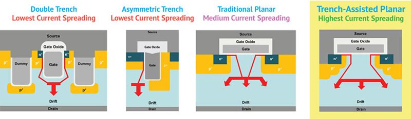
If we now look at the effect of this structure on the on resistance at high temperatures, the multi-step profile enabled by the trench-assist feature enables a better current spreading and therefore lower RDS,ON (see figure 2).
RDS,ON typically increases with temperature in MOSFETs, however this benefit is maintained even when operating at elevated temperatures, for which the trench-assisted planar design has been optimized. And by maintaining a lower RDS,ON across the operating range, conduction losses are reduced, leading to cooler operation and higher efficiency. This improved performance is partly due to the enhanced current spreading facilitated by the trench-assist's multi-step profile.
Click image to enlarge
Figure 2: Schematic view of current spreading in traditional planar double trench, asymmetric trench, traditional planar, and trench-assisted planar technologies
Thirdly, the optimized device geometry and electric field control contribute to better switching characteristics, including potentially lower switching losses.
And finally, the trench enables the ability to address a critical challenge in SiC MOSFETs: the reliability of the gate oxide. As we’ve touched on, the gate-oxide can be subjected to high electric fields at trench corners, with the trench-assisted planar design mitigating these stresses to give a more stable threshold voltage (VTH) and improved gate oxide lifetime.
Evaluating the Architecture
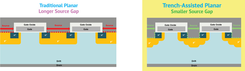
As can be seen in figure 3, the shallow trench in the source region of trench assisted-planar design provides enough surface to implement the metallization in a smaller source gap than the traditional planar approach. The effect of this is to enable a lower cell-pitch and therefore a lower RON,SP .
Click image to enlarge
Figure 3: Cross-sectional view of source region in a traditional planar (left) and trench assisted planar (right)
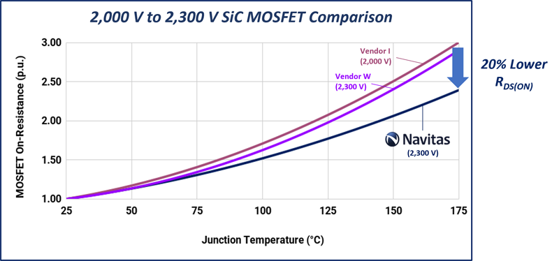
Furthermore, as a direct benefit of the optimized current spreading as shown in figure 4, RDS,ON has been shown in tests to be up to 20% lower at elevated temperatures compared to competing planar devices, resulting in lower conduction losses and cooler running.
The impact of this is significant. For a standard MOSFET, increasing from the quoted ambient temperature to a device’s maximum junction temperature (TJmax) will typically double RDS,ON. While not immune to this effect, it is significantly reduced for the trench-assisted planar architecture, with tests showing an increase of just 50%. And for comparative experiments using a 1200 V, 40 mΩ GeneSiC MOSFET housed in a D2PAK package alongside devices from other vendors under matched circuit design conditions, the trench-assisted planar device recorded a case temperature that was 25°C cooler than competing devices. Such a reduction in operating temperature translates to a three times longer operational lifetime.
Click image to enlarge
Figure 4: Normalized RDS,ON, comparison for trench-assisted planar, trench-gate and planar-gate
While RDS(ON) is a critical parameter, it is not the sole measure by which to choose a MOSFET.
Of equal importance is its behavior under high-speed switching conditions and the magnitude of the resulting energy losses. Here, the optimized electric field and reduced parasitic capacitances observed in the trench-assisted planar design also contributes to faster and more efficient high-frequency switching, enabling a higher power density and better figures of merit (FOM) for both hard-switching (EON + EOFF losses) soft-switching (EZVS losses) applications.
Technology Evolutions
Navitas's GeneSiC trench-assisted planar technology represents a significant advancement in Silicon Carbide (SiC) power MOSFET design, effectively overcoming the inherent trade-offs typically found in traditional planar and trench architectures.
By strategically incorporating shallow trenches into a fundamentally planar gate structure, Navitas delivers a "no-compromise" solution. This innovative approach ensures high-yield manufacturing and enhanced thermal dissipation with the simultaneous optimization of the electric field distribution to achieve the lowest RDS,ON at high temperatures, reduced switching losses, and superior gate oxide reliability.
R&D continues, with work to implement this structure for next generations SiC technologies and enhance the performance across the entire operating temperature for these devices. This will involve reducing the RON x Chip Area metric along with improvements in robustness needed for today’s automotive applications.
Gen5 devices will shrink the cell pitch thus reducing the RON,SP and gate charge (QG) and offer significant reductions in switching losses. The focus for Gen6 is to further lower on-resistance at elevated temperatures, with the first Gen5 devices available later this year and the first Gen6 devices available within three years.
Conclusion
The design of switched power converters is a delicate balancing act, forcing engineers to make tough choices between performance, cost, and long-term reliability.
The trench-assisted planar architecture offers a way to move beyond these compromises and by combining the strengths of both traditional planar and trench designs, this novel multi-step profile reduces the need to trade off to achieve the least-worst option. Instead, the result is a reliable and robust device that allows for higher efficiency, cooler operation, and the ability to build more compact and power-dense converters without sacrificing cost-effectiveness or reliability.