'Twisting' Atomic Materials may Convert Light into Electricity
US Army grant to UC Riverside will support the study of the science of light and its interaction with matter
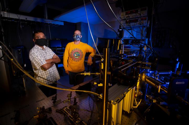
A pair of physicists at the University of California, Riverside, are aiming to convert light falling on atomically thin semiconductor materials into electricity, having received more than $582,000 in funding from the U.S. Department of the Army.
Nathaniel Gabor and Vivek Aji, both associate professors of physics and astronomy, will focus on how the fundamental science of light and its interaction with matter enables new sensing capabilities in layered and twisted vertical structures of stacked monolayer semiconductors. The researchers aim to understand how electronic excitations influence the flow of photo-absorbed energy in ultrasmall semiconducting optoelectronic materials.
"This research effort has the potential to impact fundamental science and technology, involving physics of quantum processes in light-sensing and deeper knowledge of novel optoelectronic properties in 2D quantum materials," said Tania Paskova, program manager of the U.S. Army Combat Capabilities Development Command, known as DEVCOM, Army Research Laboratory. "A successful execution will open new opportunities for quantum enhanced sensors that could usher a new era of night vision technology and quantum communication networks, both of significant importance for the Army."
Gabor and Aji expect their stacking and twisting approach will spawn a new generation of quantum photodiodes that operate at room temperature, next-generation photovoltaics, single photon sensors, and light-emitting diodes, or LEDs. They will be among the first to explore the ability to stack-engineer the interaction between vibrational motion and electronic states, heralding a new era of quantum sensor science.
"We think this project will give us a deep understanding of fast and highly sensitive quantum coherent electron-hole separation in light sensing," said Gabor, the three-year grant's principal investigator. "It also promises rapid future advancement of precisely engineered materials and devices for advanced light-sensing technologies."
Using theoretical modeling as a tool, Gabor and Aji have already begun experiments with atomically thin semiconductors tungsten diselenide and molybdenum diselenide. When such semiconductors absorb a photon, a bound electron can be freed, leaving behind an electron vacancy, or hole. As the hole behaves like an electron with positive charge, the electron and hole can attract each other to form a bound state called an exciton.
"Today, we understand better even at just the stacking level how these materials behave," said Aji, a theoretical physicist and the grant's co-principal investigator. "In twisting, you arrive at a series of 'magic angles' where certain aspects repeat. Twisting is the future in this line of research."
Gabor explained that materials scientists are now easily able to isolate individual atomically thin materials and also control how they're twisted relative to each other. Engineering the interactions in these "twistronic" materials between atomic motion and excitons, however, is challenging since the interaction strength is fixed by atomic-scale configuration and electronic structure.
"Imagine a layer of red atoms on top of a layer of blue atoms," Gabor said. "By twisting these against each other, you finely manipulate the distance between the red and blue atoms and the atoms' allowed vibrations get affected in unusual ways. As you continue to make these twists ... their behavior, in turn, becomes more complex, affecting properties such as magnetism, superconductivity, and optical effects.
"With just one layer, you have a very narrow absorption of an exciton. When you start to stack and twist the layers, you can find new ways to absorb light and efficiently generate current from it."
When stacking tungsten diselenide and molybdenum diselenide layers, an electrical field may form between them. Light shining on this stack forms a bound exciton, which is then converted directly into electrons and holes with remarkable efficiency. Gabor suspects some unique quantum mechanical effects may be occurring in the tungsten diselenide-molybdenum diselenide system. Only a few materials systems behave in this manner, he said.
"It has to do with the way the atoms are vibrating and how that interacts with light," he added. "We may be seeing vibronic physics here. The ultimate goal from the Army's perspective is to find such new ways of increasing efficiency that take advantage of quantum mechanical effects. We have a whole suite of semiconductors that behave like tungsten diselenide and molybdenum diselenide to experiment with."
Aji explained that when light is absorbed in a semiconductor, some excitation is created in the system that often dissipates away.
"But if you could control the electronic properties of the materials systematically, then you could tune the materials to respond to light in just the ways you want," he said. "The stacking and twisting of semiconducting layers allow just that."
The researchers acknowledge twisting two semiconductors against each other places their work in the "Stone Age" of this research endeavor.
"Our collaborative work so far has only scratched the surface of this vast landscape," Gabor said. "With three, four, or 10 monolayers, we have a humongous parameter space to study. The good news is we will have a lot of work to do, which should keep my lab busy for long. The bad news is with many layers it gets much harder to understand what exactly is happening."
Unlike other research groups working on stacking and twisting semiconducting materials, Gabor and Aji are interested in demonstrating devices, such as room temperature vibronic sensors, from an experimental perspective.
"We are focusing on semiconductor devices with applications in photo detection and optoelectronics," Gabor said. "These devices can theoretically operate at speeds inaccessible to LEDs and lasers, promising high-speed communication. One thing worth noting is that the experiments and theory are presently moving at the same pace in this field. This is really unusual in science. What sets us apart from other research groups is that we are already building these semiconductor devices."
Gabor and Aji will be assisted in the research by two graduate students. The project, titled "Stacking and twisting van der Waals heterostructures for ultrafast and ultrasensitive vibronic sensors," begins Sept. 1.
The University of California, Riverside (http://www.
EurekAlert!, the online, global news service operated by AAAS, the science society: https://www.eurekalert.org/pub_releases/2021-04/uoc--am043021.php