Ultra-thin DS-SMD Packages Enable Full SiC Performance With Almost no Package Limiting Parasitics

Today’s EV Motor Controller Inverters are limited by conventional power
Electric Vehicle (EV) power electronics offer the largest growth potential to the Power Semiconductor Market over the next 5-10 years. Today’s EV Motor Controller Inverters are limited by conventional power silicon (Si) IGBT and diode performance, including their higher power density, higher efficiency, lower thermal resistance and smaller/lighter Motor Controllers. SiC MOSFETs can provide higher power density and efficiency, yet with SiC power density increasing faster than its efficiency, it becomes more difficult to maintain and reduce the thermal resistance in the smaller areas. Smaller Inverters built with SMD SiC devices allow simpler mechanical and thermal hardware, further reducing the complete Motor Controller size and weight. Ultra-thin double-sided (DS) surface mount (SMD) modules can provide the required SiC electrical and thermal solutions. The DS-SMD package advantages can be optimized in 650V/650A SiC Half-Bridges (HB), which can be only 29mm x 17.5mm and 0.75mm (0.030”) thick. The smaller DS-SMD power packages can enable today’s SiC EV Motor Controllers, and ever increasing SiC power density and efficiency, and at lower costs.
Ultra-Thin DS-SMD Packaging Approach and Advantages
The approach of using new ultra-thin DS-SMD packages enable full SiC performance with virtually no package limiting parasitics. These packages eliminate redundant interfaces and terminals, and significantly reduce thermal resistance per mm2 with double-side cooling and high current connections and low profile packages. The DS-SMD packages are leadless and wirebondless, significantly reducing package inductance and resistance. The low current-loop inductance can be 0.1 to 0.20nH, reducing voltage over-shoot, losses and noise, and can lower required SiC MOSFET and diode break-down voltages. Lower BV SiC can be optimized for lower Rds(on). The compact DS-SMD architecture is ideal for paralleling power switches die, further reducing Rds(on) and increasing current capabilities. Smaller SiC die reduce CTE stresses, allowing direct die-to-Cu soldering. Grouped smaller SiC die can further reduce the thermal resistance with wider heat-cones than single large die. Smaller SiC die improve yields and minimize higher costs created by today’s SiC higher defect densities and smaller wafers. Compact DS-SMD packages enable simpler and smaller Inverter and Motor Controller architectures, by eliminating long internal leads and redundant internal electrical & thermal interfaces, and can better accommodate heatsink (and cold-plate) isolation and structure. Three compact (29mm x 17.5mm x 0.75mm) DS-SMD HB packages can create an Inverter for a 200kW EV Motor Controller.
Unique DS-SMD Module Architecture
The DS-SMD HB technology is basically a double-sided power QFN package built with a one piece leadframe. The bottom-side power die are soldered into cavities and those die are exposed at the bottom-side of the package for direct soldering to the positive and negative bus bars, while leaving the top-side of the leadframe available to solder other components like bump-chip gate-drivers and chip capacitors die This double-sided assembly approach works for smaller HEV Inverters, with integrate gate-drivers and passive components on the top-side. Even higher power EV inverters are possible by using the top surface to attach an additional top-side heatsink/cold-plate, creating a single-sided assembly with double-side heatsinks and high current external pads. The type of unique DS-SMD architecture is shown in a HB example using the proprietary mMaxPak technology.
A cross-section of that half-bridge (HB) package with double-sided cooling is shown in Figure 1A. The HB packages are soldered directly onto the positive and negative bus bars, and an output lead is soldered directly onto the top of each HB package. The package is only 0.75mm (0.030”) thick, and the top and bottom pads provide all electrical and thermal connections. Since the power SiC die are soldered into the leadframe bottom-side cavities and to the copper bus bar and output leads, there are no HB package leads or wire bonds, eliminating associated inductance and resistance. This can reduce current-loop inductance to 0.1-0.2nH, and eliminates redundant lead/terminal interfaces. The power density and inductance are further reduced by co-packaging the hi-side and low side switches in the HB package. The internal layout of the 650V/650A HB is shown in the Figure 1B X-ray View of the HB package. It demonstrates internal details and interconnects. The Figure 1B HB example uses two 8mm x 7mm SiC MOSFETs & two 4mm x 7mm SiC Diodes for both high-side and low-side switches. The high-side die drains sit directly on the positive bus and the low-side die source sit directly on the negative bus. The output terminal sits directly onto the common leadframe pads for both hi-side sources and low-side drains. The gate & sense (g/s) pad locations are shown in the Figure 1B X-ray View, but vertical structures are not shown. These will be dependent on the type of associated structure and components. Current sense leads are not shown, but when required, they may be implemented just like the g/s leads.
All power package pads are soldered directly to thebus or output leads, eliminating higher thermal resistance press contacts. The positive and negative bus provides both electrical connections, and a thermal path to the bottom-side heatsink. The output pad shown in Figure 2A provides the high-current electrical connection to one phase of the motor, and the thermal paths to the top-side heat-sink. The bottom-side positive and negative pads shown in Figure 2B provide the DC input voltage from the bus bars, and the thermal path to the bottom-side heatsink. The heavy copper bus bars and output lead provides excellent heat spreading and heat transfer from the DS-SMD packages to the heatsinks, but since they are electrical connections they must be electrically isolated from the heatsinks. The heavy copper leads also provide higher heat capacity at the die/packages, minimizes junction temperature (Tj) spikes, and reducing power die dynamic thermal resistance (Rjs) to the heatsinks/cold-plates. This maintains more uniform average junction temperature with 50% HB duty cycle at lower motor RPM.

Click image to enlarge
The isolation to heatsinks must be provided to the Inverter with DBC substrates, like aluminum nitride (AlN) or silicon nitride (Si3N4)substrates. They are placed between the power leads and the heatsinks, and ideally soldered. Since the DS-SMD package are small with SiC devices, the ceramic isolators can be much smaller than in conventional power Si IGBT modules. This minimizes breakage from CTE mismatched and mechanical stresses. Breakage of the ceramic isolators can be caused by the substrate warpage and excessively large area substrates. Smaller substrates can improve reliability and reduce ceramic costs, and thinner high-strength ceramic can further lower thermal resistance, improving the performance, especially Rds(on) and reliability. For example, if an AlN isolating ceramic thickness is reduced from 0.025” to 0.015”, and the AlN is 50% of the total thermal resistance (Rjs), the junction-to-case thermal resistance (Rjs) is reduced by 20%. This is very significant for high power EV Inverters, where we fight for an extra 1% or 2% improvement.
Other Motor Controller Advantages Enabled by DS-SMD HB and Inverter
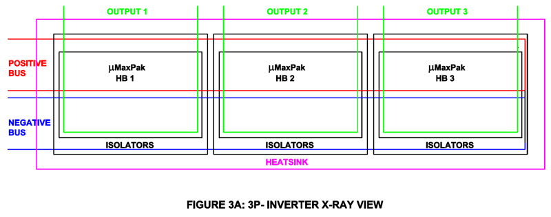
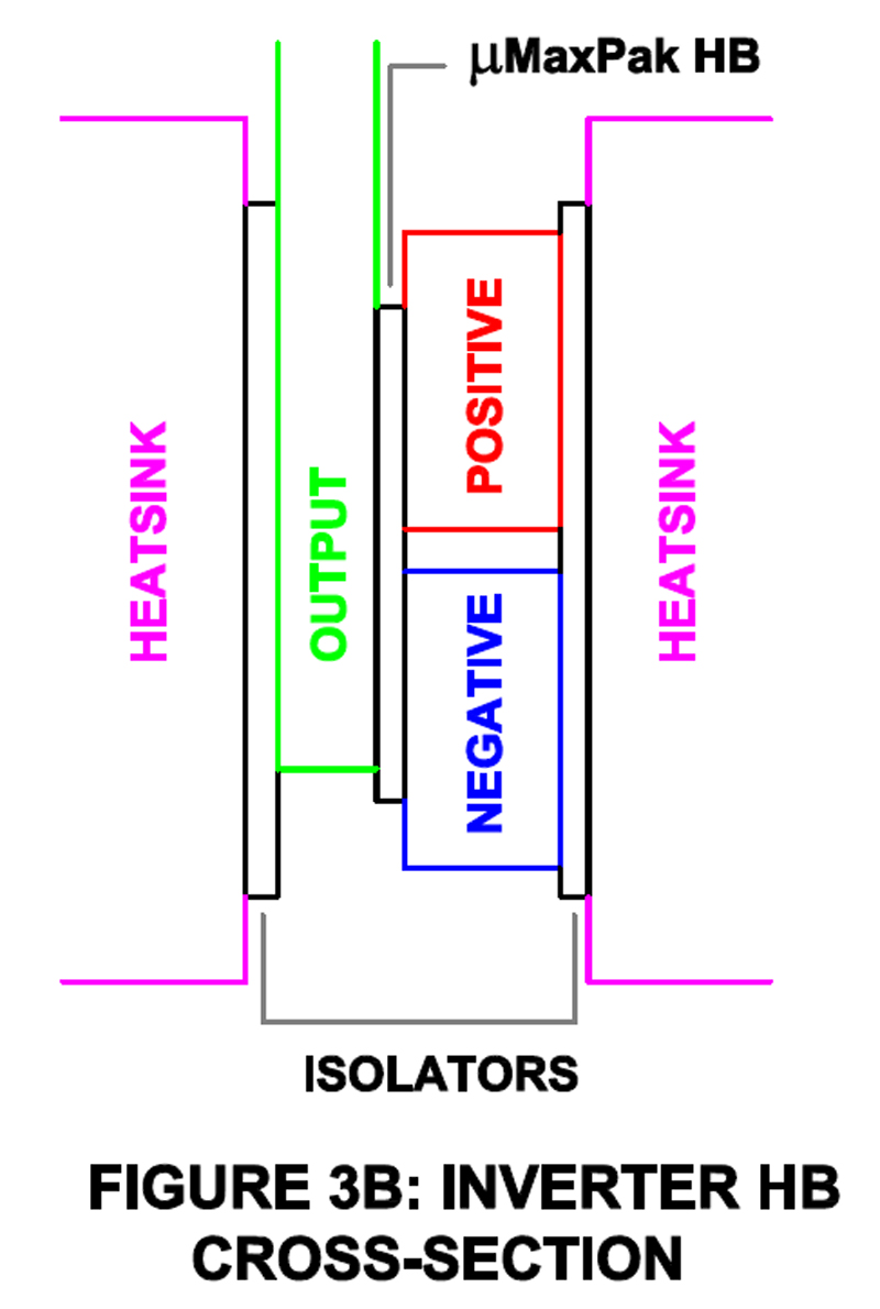
The Motor Controller structure is outside of the scope of this article, but it is important to briefly discuss how to use the DS-SMD HBs to best advantage in the Motor Controller. The exact structure will vary with power level, gate-drivers, protection circuitry, and other specific components, circuitry, functions and specifications. A basic Inverter interconnect structure is shown in Figure 3A and Figure 3B, and focuses on optimizing the electrical and thermal connections, and the locations of the DBC isolators described above.
Click image to enlarge
This optimization is essential to capitalizing on DS-SMD package driven performance, reliability and cost advantages listed below:
· Smaller SiC die and smaller DS-SMD packages make EV Motor Controller much smaller and lighter
· SiC MOSFETs and diodes can increase Motor Controller efficiency from 97 to between 99.0% and 99.5% of those built with Si IGBT modules
· With total power dissipation being reduced by a factor of greater than 3, there are proportional reductions in heatsink size and costs, and in the off-line cooling system’s size and cost
· One cannot overlook the significance of secondary performance and reliability advantages of lower operating temperatures (Tj)
· Smaller Inverters further reduce the system current-loop inductance with shorter bus-bars and interconnects, in addition to inductance reductions within the HB DS-SMD HB packages
· Reductions of Inverter’s mechanical, electrical and thermal interfaces further reduce the complete Motor Controller size and weight, improving reliability and reducing overall system costs
· Small and closer conductors and components must be managed for high-voltage spacing, which usually means potting, coating, under-fill, etc. These must meet safety agency rules and regulations, which can be better implemented inside the Motor Controller enclosure. It is important to use materials and spacing that comply with UL/EN Pollution Degree 1 regulations. These minimum HV spacings and materials may be new to PCB assembly, but have been used successfully for many years inside high power IGBT modules.
· Advantages of using thinner and smaller ceramic isolators have been described earlier, but such ceramic isolators must also be mechanically support to not create excessive pressure and twisting in the larger Motor Controller system assemblies
Summary
· High density efficient power SiC enables ultra-thin SMD modules at EV power levels
· Ultra-thin DS-SMD packages allow SiC devices to operate at their full performance and efficiency potential
· DS-SMD SiC modules are much smaller and lighter than conventional Si IGBT modules, and enable even larger reduction in the EV Motor Controller system size and weight
· Ultra-thin DS-SMD packages are built using conventional QFN technologies. This technology offers easy customization, short time-to-market, and reliable low cost packaging.