Ultrahigh power density solutions for energy-efficient high-power lighting and industrial SMPS applications

A new benchmark in 950 V superjunction (SJ) technology with an integrated fast body diode, addressing half- and full-bridge configurations
Figure 1: Gate charge
Introduction
The evolution of the industrial internet of things (IIoT) that drives the next wave of technological innovation raised the demand for high-quality and reliable industrial switch-mode power supplies (SMPS) systems that are used to power connected devices. These SMPS systems are usually operated in outdoor environments, environments without air conditioning, or systems without fans. Such operating conditions make reliability and robustness the key requirements for an industrial SMPS. Reliable supply and long-term product availability are also some critical customer concerns.
At the same time, LED lighting systems penetration has been incredibly rapid across many high-power industrial applications, such as tunnel and subway lighting, outdoor lighting, stadiums, agricultural LED plant lighting, etc. Smart LED lighting infrastructure, connected to an IoT with other sensors and actuators, enables services that create exceptional added value. Highly energy- and cost-efficient LED lights have already replaced most installations fitted with previous inefficient light sources, significantly contributing to global efforts to reduce carbon footprint and allowing for more lighting control, more consumer options, and higher-quality lighting designs.
Infineon delivers a full spectrum of innovative and high-performance LED Driver ICs and SMPS solutions with best-in-class technologies that meet all the requirements and provide the right fit for such applications. In this article, we introduce the latest CoolMOS™ 7 family, the 950 V CoolMOS™ PFD7, which fills a gap in Infineon’s high-voltage portfolio. The new technology addresses half- and full-bridge configurations, especially in the voltage class above 600 V while the wide range of products in this new portfolio offers unique flexibility to the designers.
What is new over predecessor technology
Infineon’s high voltage CoolMOS™ C3 technology was developed more than a decade ago to provide the desired high efficiency, power density, reliability, and ease of use in a wide range of applications while offering an outstanding cost/performance ratio. Technology-wise, the 900 V CoolMOS™ C3 is a direct competitor of the 950 V CoolMOS™ PFD7 and will remain on the market as a fitting solution for still some time. However, the new CoolMOS™ PFD7 family will be our future technology offering better performance and significant overall benefits compared to its predecessor. Considering also the unique range of the product portfolio, for future designs, the combination of CoolMOS™ P7 and CoolMOS™ PFD7 should be the first choice wherever possible. In light of those, this series offers the required flexibility to customers and an alternative to other competitive solutions, such as the STMicroelectronics DK5 Series, which has a more limited portfolio size.
Like the 950 V CoolMOS™ P7, the CoolMOS™ PFD7 family is easy to drive. The very low gate-source threshold voltage VGS(th) of typically 3 V and the lowest VGS(th) tolerance (±0.5 V) provide increased design freedom. Due to these tight specifications, MOSFET linear mode operation can be avoided in an easier manner, and the technology allows for a lower driving voltage and reduced idle losses.
Two relevant technology parameters, the gate charge (Qg) and the reverse recovery charge (Qrr), show the most considerable improvements over the latest generations of silicon (Si) MOSFETs.
Reducing the gate charge is crucial for increasing the light load performance. The light load performance becomes increasingly important as customers have to follow new efficiency standards resulting in the need for a light load efficiency increase in the 10 to 20 percent range of the SMPS power. The lower Qg of the seventh series CoolMOS™ MOSFETs helps to support that trend (Figure 1).
More specifically, the biggest differentiator between the former 900 V CoolMOS™ C3 technology and the already released 950 V CoolMOS™ P7 is the reverse recovery charge (Qrr). This parameter is essential for soft-switching applications since it is the main contributor to losses.
For example, under special operating conditions, in sudden duty-cycle or frequency changes, it is crucial to reduce the generated losses due to the reverse recovery charge (Qrr) to avoid thermal problems.
Comparing these parameters of the main 900 V and 950 V SJ MOSFETs competitors to the latest 950 V CoolMOS™ PFD7, it is evident that the 950 V CoolMOS™ PFD7 outperforms the internal and external competition in terms of commutation ruggedness and reliability (Figure 2).

Click image to enlarge
Figure 2: IPW95R130PFD7 trr and Qr
Moreover, for a 130 mΩ device, the 950 V CoolMOS™ PFD7 showcases about 50 percent lower Qrr, 15 percent reduced trr and 10 percent lower Irrm compared to the main competitor, the STM DK5 series. These numbers are even greater when compared to the previous technology, the 900 V CoolMOS™ C3, where the 950 V CoolMOS™ PFD7 demonstrates around 90 percent lower Qrr, as well as 80 percent lower trr, and Irrm. This is quite a big technology improvement step that limits soft switching application losses to a lower level.
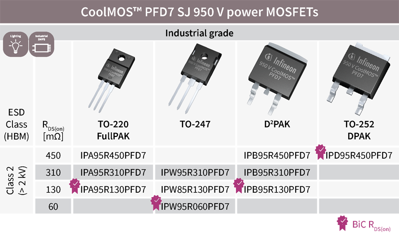
A broad portfolio size with an unmatched range of features
The 950 V CoolMOS™ PFD7 technology addresses higher-power consumer applications, which need a PFC plus a PWM stage. It represents a further upgrade of the existing 950 V CoolMOS™ P7 product portfolio with respect to the RDS(on) classes while offering the most relevant packages for mid- to high-power applications. Both families will co-exist and together smoothly replace the 900 V CoolMOS™ C3 in the following years.
The 950 CoolMOS™ PFD7 portfolio covers four packages, two through-hole (THD) and two surface-mount (SMD) packages, in four RDS(on) classes, ranging from 450 mΩ down to 60 mΩ. This range offers an excellent vehicle to address lighting and industrial SMPS applications where the focus is on the best-in-class RDS(on). The 950 V CoolMOS™ PFD7 builds on the features of the 950 V CoolMOS™ P7 and therefore offers significantly lower RDS(on) than the competition. Both DPAK and TO247 support the trend of higher power density. On top of these, a D2PAK package with 130 mΩ best-in-class (BiC) is also new in the portfolio, which was not possible with former CoolMOS™ generations (Figure 3).
Click image to enlarge
Figure 3: 950 V PFD7 portfolio
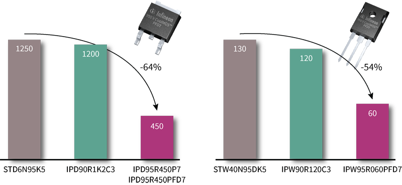
Supporting the evolution in the SMPS industry, where the newer designs are moving from through-hole devices (THD) to surface mount devices (SMD), the 950 V CoolMOS™ PFD7 portfolio offers the flexibility to make a suitable choice. A best-in-class DPAK package with a 60 percent RDS(on) reduction compared to the competition is possible. In addition, a 50 percent reduction when using TO247 packages can support the trends of higher power density and a reduction of the component count since a single device can be used instead of paralleling MOSFETs (Figure 4).
Click image to enlarge
Figure 4: Best-in-class RDSon for DPAK and TO247
Application testing and performance results
Having discussed the features, this section presents how these contribute to better system performance. The 950 V CoolMOS™ PFD7 can be used in LLC, and ZVS topologies, showing the benefits of reduced gate charge (Qg) and reverse recovery charge (Qrr) losses.
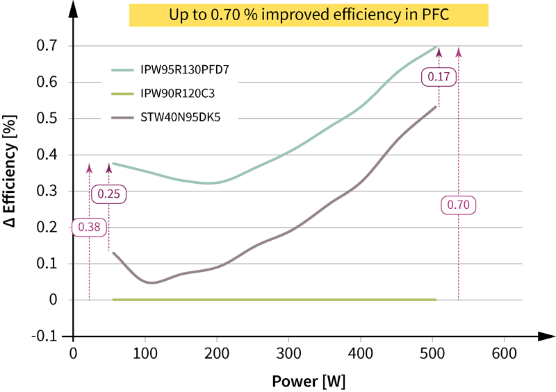
At the same time, it can also be used in PFC stages. Figure 5 shows an Infineon PFC measurement where it is clearly evident that the 950 V CoolMOS™ PFD7 outperforms previous CoolMOS™ families as well as the main competition. In fact, it offers up to 0.25 percent better light load efficiency and up to 0.17 percent improved full load efficiency over the competitor device. Compared to the predecessor 900 V CoolMOS™ C3, up to 0.38 percent light load and 0.70 percent full load efficiency is demonstrated.
Click image to enlarge
Figure 5: Efficiency measurements
A unique high-voltage control IC for one-package system solutions
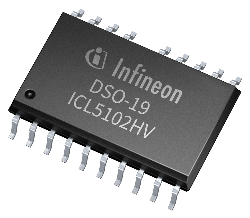
Along with the new MOSFET devices, Infineon Technologies offers a special high-voltage controller to facilitate the implementation of a high-performance full-system solution. The ICL5102HV is an integrated two-stage controller for LED drivers and comes in a DSO-19 package (Figure 6).
Click image to enlarge
Figure 6: Infineon package DSO-19 ICL5102HV controller for- led-drivers
Reducing the number of ICs to one, the ICL5102HV, a combo controller for PFC plus resonant half-bridge topology, is the perfect fit to complete and simplify the customer design, allowing shortening the time-to-market overall. Its wide variety of features and functions allows the designers to choose the best-fitting part for the application and desired topology.
It can be broadly used for LED lighting and other SMPS applications where the system bill-of-material (BOM) cost, input power quality, power density, standby power, and product reliability are critical design parameters.
Thanks to Infineon’s coreless transformer technology, the half-bridge switching frequency could be up to 500 kHz without a significant temperature increase. Driving both high- and low-side MOSFETs, non-overlap dead time is self-adaptive from 300-750 ns, ensuring compliant electromagnetic interference (EMI) behavior and high efficiency.
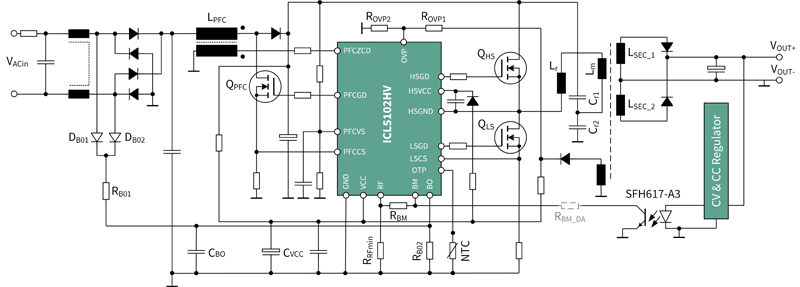
Additionally, this controller enables universal AC input voltage from 90 to 480 V. The DSO-19 package of ICL5102HV supports the capability of handling up to 980 V between high-side ground and ground (Figure 7).
Click image to enlarge
Figure 7: Schematic LLC ICL5102
Summary
The 950 V CoolMOS™ PFD7 high-voltage MOSFET series builds on Infineon’s know-how of more than 20 years in superjunction (SJ) MOSFET technology and the CoolMOS™ P7 power MOSFET family unique features. The new series adds an integrated fast body diode with ultra-low reverse recovery charge Qrr offering hard commutation ruggedness and reliability. This makes it the most robust SJ MOSFET in this voltage class, enabling usage across all topologies in the targeted applications.
In addition, the new family of products offers best-in-class figures of merit in terms of RDS(on) x Eoss, reduced Qg, Ciss, and Coss, as well as best-in-class RDS(on) in various packages. These features enable designers to support higher power density designs, substantial bill-of-material (BOM) savings, lower assembly cost, improved efficiency, and up to 4°C lower MOSFET temperature compared to the 900 V CoolMOS C3 SJ MOSFET.
The ESD protection of up to HBM Class 2 contributes to an improved production yield as ESD-related failures on the customer side get reduced. The well-known best-in-class quality and reliability of the CoolMOS™ 7 families again support fewer issues in production and reduced field returns.
Last but not least, the 950 V CoolMOS™ PFD7 allows price competitiveness over the 900 V CoolMOS™ C3 family, which enables cost-competitive SMPS designs on the customer side by offering a long-term price roadmap.
For more information on this new technology and product portfolio, click here.