Understanding Common-Mode Noise in Low-Power Offline Supplies
Offline supplies for mobile phones need to be simple, low cost, and highly efficient power converters
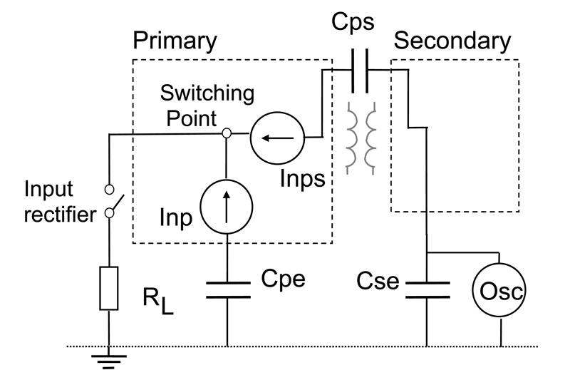
Figure 1. A flyback converter's main common-mode noise sources and transfer paths.
Yet the ruggedness of the underlying technology makes the core designs attractive to a much wider audience, such as industrial users who need low-power supplies for DIN-rail and similar equipment. But while industrial applications stress long-term reliability over cost and have few constraints on form factor, minimal cost and size are essential in the consumer space. EMI suppression then becomes very difficult, with no Earth connection or X/Y capacitors, few input-filter components, and arbitrary power-cable lengths. Methods exist to mitigate these issues, but rarely in isolation from other contributors. For instance, twisting the power cable's conductors theoretically makes length less critical. But as any EMC test engineer knows, cable length and layout heavily influence results. At another level, a modified topology such as the resonant discontinuous forward converter (e.g. CamSemi C2470 controller family) that softens primary-side switching eases meeting regulatory requirements with minimal EMI-filter hardware. Applicable standards include EN 55022 for conducted and radiated emissions, and ETSI EN 301 489-34 for conditions that apply to mobile phone chargers as defined by IEC 62684. Yet the touchscreens in today's smartphones are highly susceptible to noise that can be present at a supply's output. Typically, this becomes apparent when using the phone during a charging cycle. Connections to ac-line create a competing noise current path that may swamp the user's connection to Earth, which the touchscreen relies upon for sensing user inputs. Due to consumer requests for a common charger that suits all data-enabled mobile phones, the �MoU initiative' targets interoperability issues and the environmental impact that results from disposing of countless special-to-type chargers [see http://ec.europa.eu/enterprise/sectors/rtte/chargers/docs/index_en.htm]. Because common-mode noise affects different touchscreens to varying extents, resolving this issue is crucial for interoperability. Currently in its first edition, IEC 62684 is the MoU initiative's standard for ensuring interoperability between phone-charger power supplies. It specifies criteria such as universal-input ac-line operation, USB Micro-B cabling, compatibility with the USB-IF standard for device-detection and protection, environmental operating conditions, and the charger's dc output characteristics. This last section states that the output voltage shall be 5.00�0.25 VDC from no load to a full output current level that must lie between 500 and 1,500 mA. It also lays the foundation for common-mode noise limits and demands some specific tests. Mechanisms that create common-mode noise The flyback topology dominates low-power ac/dc conversion as it is simple, efficient, and inexpensive. We will consider two periods within any switching cycle - the �charge' period during which energy builds in the transformer's core, and the 'discharge' period while this energy releases into the secondary circuit. The common-mode noise waveform at the dc output differs substantially during the Bridge Conduction Time (BCT period) when the input rectifier is conducting from the remainder of the ac-line cycle, when it is non-conducting (Bridge Non Conduction Time, BNT). With the switch on the left-hand side of figure 1 representing the input rectifier, we see the two circuits that operate during these periods:
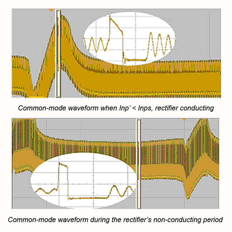
During the BCT period, the switch connects the transformer's primary to ground, causing a common-mode noise current Inps to flow between the secondary and primary to become the dominant noise term. The common-mode signal that results at the charger's output is proportional to the difference between Inps and Inp, which is the noise current that transfers from primary to Earth. There are two possible conditions: Inp > Inps—the resulting waveform is the same shape as the switching signal Inp < Inps—the waveform is proportional to the inverted switching signal—see the top trace in figure 2. As the bottom trace in figure 2 shows, the waveform during the BNT interval will always be the inverted switching signal, as the main noise source is the primary pushing current to Earth through capacitor Cpe. The main switching components differ between the BCT and BNT periods together with the high-frequency signal content. Because the largest peak-to-peak voltage Vpp can appear anywhere in the ac-line cycle, quantifying Vpp demands identifying the worst-case levels in multiple frequency bands. The key to optimizing conducted emissions lies with precisely balancing the two conditions during the BCT period.
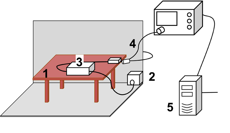
Test configuration set-up Common-mode noise measurement accuracy depends on test method and setup. To test the external power supply (EPS), we use the set-up that EN 55022 defines together with these modifications from IEC 62684:
- 30 cm distance from the EPS cables, loads, and mobile terminal to Earth
- 10.00 � 0.01 ? load
- EPS powered by 253 VAC -1% / +0% at 50 Hz � 1%
- 1 m cable from EPS to the load.
- Non-conductive table
- LISN and EPS supply cable
- EPS, output cable, and mobile terminal
- 8 pF/10 M? probe to the oscilloscope
- Computer
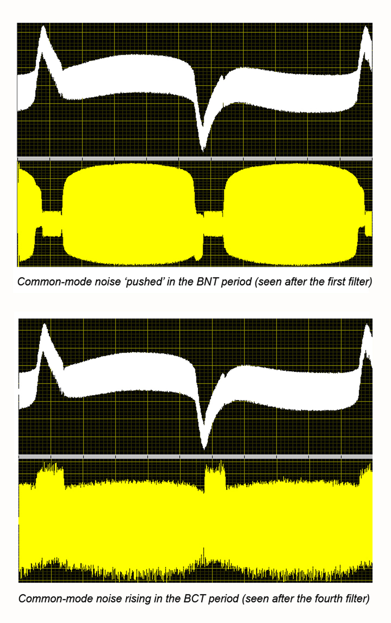
Measurement method An objective within IEC 62684 is to measure the worst-case Vpp signal amplitude over a 20 msec ac-line cycle at 253 VAC, as common-mode noise tends to worsen at high input voltages. CamSemi's approach exploits a digital oscilloscope to acquire the line-frequency signal frame in four million samples. This data passes through digital filters and frame-scan measurements to find the worst Vpp signal in each frequency band. Recently, the MoU initiative published a "Guide on Implementation of Requirements of the Common EPS" to support IEC 62684: The Guide exempts many of the common-mode noise tests in IEC 62684, recommending instead measurement of all pulses longer than 250 nsec. This effectively results in a single frequency band from below the switching frequency to 4 MHz. Test results and possible compensation strategies Examining the common-mode noise shapes and amplitudes after filtering can help identify interference sources and suggest approaches to mitigating the problem. A two-stage approach minimizes noise at source before applying a signal of opposite phase and amplitude to the remaining noise signal. A range of suitable mechanisms for achieving this are discussed in CamSemi US patent 8,023,294 www.google.com.tr/patents/US8023294. Compensation methods include balancing the transformer's design to "push" noise between BCT and BNT periods. The top traces in figure 4 show the result of pushing the common-mode noise signal during the BNT period. All compensation methods suffer from signal inaccuracies that worsen as frequency increases. The relationship between the signals in the high-frequency area can be completely different from the main switching frequency band, and the extent of the difference within this relationship is one measure of the quality of the compensation. The bottom traces in figure 4 show the 1 to 100 kHz and 1 to 100 MHz frequency bands for the same signal, revealing the onset of increasing common-mode noise during the BCT period due to signal delays and inequalities in compensation. Conclusion While it may not necessarily optimize conducted emissions - adjusting the compensation to drive the signal amplitudes during the BCT and BNT periods to being as close to equality as possible is the best method for minimizing common-mode noise. www.camsemi.com


