GaN ICs simplify designs, improve performance and boost robustness & reliability
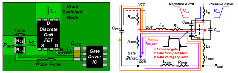
Figure 1a: Discrete GaN FET on PCB and ‘hidden’ parasitic resonant network with switching current paths
GaNFastPower ICs have enabled 10x higher switching frequencies versus Silicon and achieved unprecedented power densities (1.3 W/cc) due to their integrated and regulated gate drive technology. Discrete GaN FETs continue to have slow adoption due to ruggedness & reliability concerns, plus difficulties with designing robust gate drive circuits. In addition to very low ESD tolerance, the exposed gate of the discrete GaN FET has a high susceptibility to device, package and PCB parasitics. These ‘hidden’ parasitics are the well-known enemy of fast switching and can cause transient ringing, glitching and destruction. Unregulated on- and off-state gate voltage levels are also concerning due to wide voltage variations that can cause poor reliability and drastically reduce lifetime. As a result, discrete GaN FET solutions must add large filter circuits that prevent high frequency operation and prohibit the benefits of GaN. With GaNFastTM Power ICs, the GaN power FET, gate drive circuit and gate voltage regulator are monolithically-integrated on the same IC chip. These circuit blocks provide excellent immunity against switching noise and parasitics, eliminates gate voltage variations, and delivers a rugged and robust solution that is easy-to-use and unlocks high frequency operation for next generation power-supply designs. This article exposes these ‘hidden’ parasitics, explains why they are concerning, and compares the robustness and reliability of exposed gate discrete GaN approaches versus GaNFastTM integrated gate drive solutions during different switching conditions.
Hidden Resonant Parasitic Network
For enhancement-mode (eMode, normally off) discrete GaN FETs, a high level of sensitivity exists at the gate due to a low threshold voltage and a narrow gate voltage operating range. To make things worse, there is a ‘hidden’ resonant network of parasitic resistors, inductors and capacitors around the FET formed by the PCB, GaN FET package, and GaN device itself. An example of this parasitic resonant network consists of a discrete GaN FET mounted on a standard FR4 PCB (Figure 1a). This ‘deceptively simple’ circuit seems like it will easily work for generating the necessary square-wave gate voltage. A more detailed ‘extracted’ circuit including parasitics reveals a much more complex network surrounding the discrete GaN FET. PCB material, PCB copper traces, GaN FET package leadframe and wirebonds, and external component parasitics all form parasitic resistors, inductors and capacitors at the gate, drain and source. The intrinsic capacitors of the GaN FET device itself (CGS, CGD, CDS) also form part of the parasitic network.
Click image to enlarge
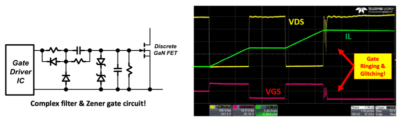
Figure 1b: Complex filter and Zener gate circuit, and, gate voltage ringing and glitching waveforms
This parasitic resonant network becomes excited during each dV/dt switching transition of the drain voltage causing currents to flow around various parasitic resonant circuit loops. These resonant currents (Figure 1a) will cause excessive voltage spikes and ringing to occur at different parasitic circuit nodes, including the gate of the GaN FET. During turn-on, a negative dV/dt occurs at the drain node causing current to flow into the gate node and through CGD to the drain. During turn-off, a positive dV/dt occurs at the drain node causing current to flow through CGD and out of the gate node. The external gate drive signal itself will also excite the gate and source loop parasitics. All of these switching conditions will cause voltage spikes and ringing (Figure 1b) at the gate that will turn the discrete GaN FET on or off unexpectedly (glitching) and can cause poor reliability, reduced lifetime or destruction of the GaN FET. These constraints make these devices very susceptible to high-frequency and high dv/dt noise from the surrounding switched-mode converter circuit. To mitigate these problems, external components are placed at the gate that include a gate capacitor to filter the voltage spikes, a series capacitor and Zener diodes to generate positive and negative gate voltage levels, and additional resistors to help dampen the gate ringing induced by the gate loop inductance (Figure 1b). Adding external components will not completely eliminate these problems due to component tolerances, temperature variation, and internal package parasitics, so the internal gate of the device can still have spikes and ringing even if the external gate pin waveform looks clean. Also, the gate is still exposed on the PCB making it always susceptible to external voltage surges and transients, or dV/dt occurring elsewhere in the circuit, creating high risk for field failures. Dealing with all these problems, while trying to increase switching frequency and increase power density, can be a major roadblock to bringing a product out of the lab, into production, and into the field. A simpler and more reliable solution is needed without adding additional design difficulties or robustness concerns.
Integrate the Gate
It is well known that GaN offers the ability to integrate additional circuits monolithically on the same IC as the power device, so it makes good sense to include the gate drive circuitry in order to eliminate these external gate drive challenges. GaNFastTM Power ICs integrate the GaN power FET together with the gate driver, the gate voltage regulator, and voltage reference (Figure 2). During turn-on, current flowing through CGD due to the negative dV/dt at the drain no longer flows through the gate loop as it does with external gate drive circuits and exposed gates. Instead, the current flows from gate drive supply voltage (VDD), through the pull-up transistor of the gate driver, and through CGD to the drain. During turn-off, current flowing through CGD due to the positive dV/dt at the drain flows through the pull-down transistor of the gate driver and then to the source. The sink and source currents are supplied on-chip directly from the gate drive supply voltage (VDD), not from the external gate driver as with discrete GaN FETs. The integrate gate drive circuit bypasses the external gate drive loop completely and eliminates gate voltage spikes and ringing. The gate voltage is now decoupled from the parasitic resonant network and has well- controlled on and off voltage levels that are unaffected by PCB and package parasitics, component tolerances, temperature variations, and external surge or burst transient conditions. GaNFastTM Power ICs also include programmable dV/dt control and a wide-range supply voltage input (VCC) that makes them highly flexible and compatible with many popular power supply controllers on the market.

Click image to enlarge
Figure 2: GaNFastPower IC with integrated gate, no gate loop parasitics, and no ringing or glitching
GaNSenseTechnology
The latest Navitas GaNFastTM Power IC product family now includes GaNSenseTM technology. GaNSenseTM technology strengthens immunity against parasitics, voltage spikes and ringing even further by integrating loss-less current sensing. By integrating the current sensing function into the IC (Figure 3), the external current-sensing resistors, typically placed between the discrete GaN FET Source and PGND, are now eliminated. This eliminates the parasitic inductance typically formed by the PCB trace connecting the Source to the external current sensing resistor, and the current sensing resistor itself, that can also cause gate voltage spikes and ringing with discrete GaN FETs. This gives further decoupling of parasitics from the GaNFastTM Power IC resulting in even more robust and reliable switching performance without the need for additional filter components or bead inductors to suppress ringing and slow down the switching frequency. Removing the external current sensing resistors also increases system efficiency by +0.5% and removes a PCB hotspot (typically > 85C). GaNSenseTM technology also includes additional protection features such as over-current protection and over-temperature protection, making it the most robust, reliable and efficient solution available today.

Click image to enlarge
Figure 3: GaNSensetechnology integrates loss-less current sensing and eliminates source loop parasitics
Avoid the Danger Zones!
The GaN FET gate voltage levels (transient and continuous) during each on and off period are also critical for proper robustness and reliability. During the on-time period, the ‘on’ gate voltage level must stay above a minimum value (6V) to prevent RDSON from increasing, and, must stay below a maximum value (7V) to prevent accelerated lifetime degradation or destruction of the gate. During the off-time period, the ‘off’ gate voltage level (GND) must stay a safe margin away from the gate threshold level (1V) to prevent false turn-on and must not go below a maximum negative voltage rating to prevent destruction (-20V). To avoid these danger zones (Figure 4), the gate voltage levels must be well controlled at all times and should not have excessive variation over tolerances and temperature. External gate drive components used to control the gate voltage of discrete GaN FETs will still exhibit voltage spikes and will vary with temperature. Both plateau or transient gate voltage levels in the upper danger zone area will have a dramatic effect on reliability and will cause the lifetime of the device to degrade rapidly (as can be seen by the logarithmic scale of the y-axis for time-to-fail, Figure 4). The integrated voltage regulator of the GaNFastTM Power IC ensures that the voltage levels always stay within a safe range (6 to 7V), and the integrated gate driver prevents gate voltage spikes from entering these danger zones resulting in excellent reliability and lifetime.

Click image to enlarge
Figure 4: Gate voltage danger zones and gate voltage vs lifetime graph
Conclusion
GaNFastPower ICs, with integrated drive, control and protection, enable the design of next generation high-density power converters without the difficulties associated with high-frequency switching environments, ‘hidden’ parasitic networks, and gate drive ringing and glitching. The parasitic gate and source loops have been completely eliminated to prevent gate voltage spikes, and the gate voltage levels are well-controlled in order to achieve excellent reliability and lifetime standards. Integration of loss-less current sensing increases system efficiency and eliminates hot spots, and integrated protection features provide fast and autonomous immunity against over-current and over- temperature fault conditions. Frequencies are being pushed higher in order to increase power density so there is very little switching time available for slowing down and filtering the gate against voltage spikes. The exposed gate will always have a risk due to transients coupling into the parasitic network through some unforeseen circuit path. ESD can also be a big concern for discrete eMode GaN FETs. 40 million parts shipped without field failure give evidence that it is best to integrate the gate drive, increase robustness and reliability, and go GaNFast!


