What is the problem?
With USB being a standard interface in PC peripherals, the number of applications that can be powered from a USB port is increasing at an exponential rate. The need for flexibility and continuous connectivity in our lives is becoming more important than ever before. In a growing wireless world, many applications are taking portable form allowing users the ease and flexibility of connecting to the web anywhere, anytime. With all the benefits this brings, there are a number of extra requirements that need to be taken into account when designing a device that is powered from a USB port.
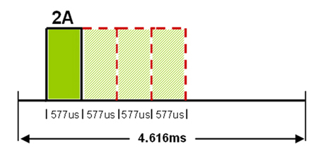
A growing variety of wireless data cards for applications such as GSM, GPRS or WiMAX data communication use TDMA techniques which require peak current during the transmission of signals which can exceed the maximum current specified by the USB standard. Therefore the modem must be designed to limit the input power and draw on card-based storage for most of the energy requirement during a typical transmission cycle. As shown in Figure 1, the GSM signal is transmitted over the carrier at a rate of 216 Hz (4.616ms pulse repetition interval). The transmission period is divided into eight time slots and depending on the power class being used (8, 10 or 12) , the duty cycle of this high current pulse can range anywhere between one-eighth of the cycle (577us) up to half of the transmission cycle (2.308ms).
Much of the work in GSM power supply design revolves around the transmission cycle due to the high current consumption in this mode. The main problem with the GSM or GPRS requirement is that in datacard applications, the average input current being drawn at the USB host is between 500mA - 700mA, while most transmitters will need 1.5A to 2A peak bursts to transmit at full power. For example, when transmitting in GPRS Class 10, a maximum of two of the eight 577?s slots are used, while the remaining 6 slots are used to recharge the capacitor, during which the supply current is reduced to less than 100mA. Therefore the power supply must be able to supply at least the average current over one transmission period, as well as be capable of handling the 2A transmission bursts. Clearly it is not possible for a power supply needed for a USB data card to operate correctly without any special design measures.
There are numerous different topologies which can be used to power a wireless datacard. But for the purpose of this article we will compare a Buck Converter Only option versus that of using a Current Limit Switch and Buck Converter combination to demonstrate the significant savings a designer can achieve by using the latter.
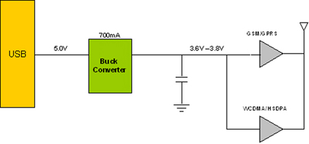
Taking a look at figure 2, this provides us with the smallest converter size due to the use of only one buck converter. But due to the fact that 2A transmission pulses still need to be buffered, a large and expensive capacitor is required. Assuming that the DCDC has an input current of around 700mA, with the supply voltage directly from the USB port (i.e. 5V) and an output supply for the RFPA of 3.8V, allows us to effectively supply around 920mA directly from the DCDC converter (no switching losses taken into account).
 The rest of the energy for a GSM transmission slot needs to come from the capacitor.
ICAP = IGSM - IDCDC
ICAP = 2.0A - 920mA = 1.08A
Therefore the effective capacitance required to buffer each pulse assuming class 10 transmission (1.154ms slot) is equal to:
The rest of the energy for a GSM transmission slot needs to come from the capacitor.
ICAP = IGSM - IDCDC
ICAP = 2.0A - 920mA = 1.08A
Therefore the effective capacitance required to buffer each pulse assuming class 10 transmission (1.154ms slot) is equal to:

 But as in many new applications, form factor and low price are firm requirements. And with the datacards this is no different. Newer models are being incorporated into small USB sticks which integrate small displays as well as the ability to add Micro SD flash memory.
This really constrains the amount of space available for electronic components, therefore using a large capacitor complicates layout of the design if space is restricted and is generally more expensive.
New Approach - Why store energy at higher voltages?
Taking both the requirements of size and price into account, there are alternative options to save on the bulk capacitor. By increasing the energy in the capacitor, the designer can drastically reduce the effective capacitance required, thereby reducing total solution size as well as costs!
The energy stored in capacitors is related to the charge at each interface, q (Coulombs), and potential difference, V (Volts), between the electrodes. The energy, E (Joules), stored in a capacitor with capacitance C (Farads) is given by the following formula:
But as in many new applications, form factor and low price are firm requirements. And with the datacards this is no different. Newer models are being incorporated into small USB sticks which integrate small displays as well as the ability to add Micro SD flash memory.
This really constrains the amount of space available for electronic components, therefore using a large capacitor complicates layout of the design if space is restricted and is generally more expensive.
New Approach - Why store energy at higher voltages?
Taking both the requirements of size and price into account, there are alternative options to save on the bulk capacitor. By increasing the energy in the capacitor, the designer can drastically reduce the effective capacitance required, thereby reducing total solution size as well as costs!
The energy stored in capacitors is related to the charge at each interface, q (Coulombs), and potential difference, V (Volts), between the electrodes. The energy, E (Joules), stored in a capacitor with capacitance C (Farads) is given by the following formula:
 Therefore the capacitance required is a function of the voltage squared. Hence the higher the bias voltage on the capacitor, the more energy stored which means you can reduce the total effective capacitance and still achieve the same amount of energy required to buffer a transmission load pulse.
To illustrate this topology, we used a current limit switch and buck converter from Texas Instruments.� The figure below shows how this topology can be implemented by using DCDC converters from Texas Instruments'.
Therefore the capacitance required is a function of the voltage squared. Hence the higher the bias voltage on the capacitor, the more energy stored which means you can reduce the total effective capacitance and still achieve the same amount of energy required to buffer a transmission load pulse.
To illustrate this topology, we used a current limit switch and buck converter from Texas Instruments.� The figure below shows how this topology can be implemented by using DCDC converters from Texas Instruments'.
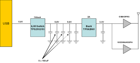
The TPS2552/53 USB power-distribution switches from Texas Instruments as intended for applications where precision current limiting is required or heavy capacitance loads and short circuits are encountered. These devices offer a programmable current-limit threshold up to 1.5A via an external resistor with accuracy as tight as �6% at higher current limit settings.
The TPS62065 is a 3MHz high efficient step-down converter used as the post regulator to supply the 2A current pulses required by the RFPA during the transmission cycle. For low noise applications, the device can be forced into fixed frequency PWM mode by pulling the MODE pin high. The TPS62065 is available in a 2x2 QFN package.
Due to the total size restriction, low profile bulk buffer capacitors are required to supply the energy to the load and maintain the output voltage within the specified limits during the high current pulses. Here, three small 150?F, low profile, Sanyo POSCAP solid tantalum capacitors are used to provide power to the load during pulsed load events. Given the magnitude and the duration of the pulsed load current, the capacitors are chosen to meet the maximum input voltage droop of the step down converter (VIN_MIN = 3.5V), while still maintaining a stable 3.3V supply to the RFPA.
The voltage drop in the circuit comprises two components, the IR drop associated with the capacitor's internal resistance (as approximated by ESR) and the drop in capacitor voltage at the end of the pulse. Neglecting the input current supplied by the source, the total output voltage droop is given by:
 Where VDROOP is the change in output voltage, IPULSE and tPULSE are the peak pulse current and duration respectively, RESR is the capacitor ESR and COUT is the output capacitance.
This energy storage benefit can be shown by comparing two different scenarios. As shown in the comparison below, two different bias voltages were applied to the buffer capacitor and the energy stored in the capacitor, as well as the total effective capacitance required has been calculated. For the purpose of the calculation we have used a Class 10 (1.154ms) transmission pulse.
Where VDROOP is the change in output voltage, IPULSE and tPULSE are the peak pulse current and duration respectively, RESR is the capacitor ESR and COUT is the output capacitance.
This energy storage benefit can be shown by comparing two different scenarios. As shown in the comparison below, two different bias voltages were applied to the buffer capacitor and the energy stored in the capacitor, as well as the total effective capacitance required has been calculated. For the purpose of the calculation we have used a Class 10 (1.154ms) transmission pulse.
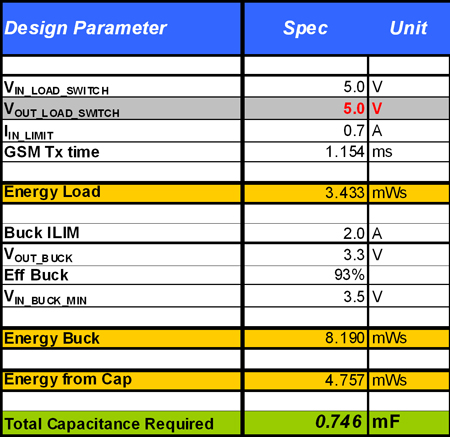
To calculate the total capacitance required to buffer a transmission pulse, requires that we understand how much energy the intermediate capacitors are charged up with and how much the buck converter needs to power the RFPA during transmission. Taking these numbers into account, we can calculate how much energy is required from the capacitor and as a result the total capacitance required:
 As can be seen in Table 1 and the calculations above, both comparisons have a significant advantage due to the total reduction in capacitance compared to that of the stand alone buck converter, while still maintaining the total required energy in the capacitor.
The energy that the TPS2552/53 supplies at a higher voltage effectively reduces the total capacitance. This in turn significantly reduces costs and solution size.
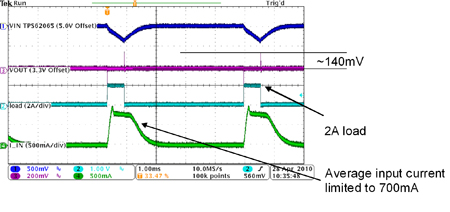
Figures 4 and 5 show screen plots of the TPS2553 + TPS62065 configuration, which uses 5 x 150uF (Sanyo POSCAP) as buffer stage, while being loaded with typical 2A pulses at power class 8 and 10 respectively (577us and 1.154ms). During the period where no transmission occurs, little or no current is being drawn from the device and the output voltage remains stable at 3.3V. As soon as a load pulse is applied during transmission, the output voltage of the current limit switch starts to droop while the required power level is supplied to the load, and the output of the buck remains stable during each transmission period.
As can be seen in Table 1 and the calculations above, both comparisons have a significant advantage due to the total reduction in capacitance compared to that of the stand alone buck converter, while still maintaining the total required energy in the capacitor.
The energy that the TPS2552/53 supplies at a higher voltage effectively reduces the total capacitance. This in turn significantly reduces costs and solution size.
Figures 4 and 5 show screen plots of the TPS2553 + TPS62065 configuration, which uses 5 x 150uF (Sanyo POSCAP) as buffer stage, while being loaded with typical 2A pulses at power class 8 and 10 respectively (577us and 1.154ms). During the period where no transmission occurs, little or no current is being drawn from the device and the output voltage remains stable at 3.3V. As soon as a load pulse is applied during transmission, the output voltage of the current limit switch starts to droop while the required power level is supplied to the load, and the output of the buck remains stable during each transmission period.

Until recently, designers of portable systems have rarely used large capacitors for applications other than back-up or standby functions where currents are low and charge times are fairly long. But a growing range of new applications, led by a new generation of high performance data cards, demand high peak currents that are forcing designers to consider new solutions. In these applications, designers are frequently looking for different approaches to reduce charge time, solution size and total cost, while still being able to deliver the high required peak currents. The compact solution using the TPS2553 USB power-switch and TPS62065 2A step-down converter from Texas Instruments is an optimal GSM/GPRS power supply solution for USB powered peripherals. Its small solution footprint, combined with today's low profile tantalum capacitors elegantly solves the pulsed load problem, providing a cost-effective, compact solution. www.ti.com