A dual-output gate driver SPICE model
This article is Part One of a mini-series, presenting useful SPICE model blocks to help motor control and power supply designers perform effective simulations. Brushless DC motors are appearing in more medical equipment these days, and designers in that industry are replacing older technologies and learning new ones. Small brushed DC motors are appearing with half-bridge circuits driven by microcontrollers. Circuits and application notes are readily available for half-bridge configurations needed to drive motors and power supplies.
Modeling these circuits is a different story. Power supply designs in medical and consumer applications are becoming more specific. Each design must meet critical needs of efficiency, space, and cost. Previously, the one-size-fits-all approach worked, but efforts are now in place to squeeze the last few pennies or the last few efficiency percentage points out of these designs.
More design engineers are utilizing circuit simulations of various types, to cut time to market and to get things right the first time, saving additional time and cost. Many vendors have created online tools for analyzing the benefits of whatever items they are selling: IGBT’s, MOSFET’s, Motor Controllers, PWM IC’s, etc. Yes, my friends, the free online tools are advertising. But you knew that.
Using traditional SPICE tools (such as Multisim by National Instruments) to simulate power supply or motor control circuits can be quite challenging without the proper building blocks available. Visiting every vendor homepage trying to compare brands and techniques is quite complex without one standard platform on your own PC.
For those of us that love to simulate, we know what a joy it is when a “block” or SPICE model is tested and available, ready to drop into our schematic so that we can continue to work on the circuit at hand, to solve and analyze our immediate needs. Without these tested blocks, we end up troubleshooting our models instead of our circuit. We need simulation models that converge cleanly, run quickly, and have been previously proven.
The typical application circuit is shown in Figure 1. DUALCLOCK generates two out-of-phase, differential, floating clock outputs, with programmable slewrate and deadtime. DUALCLOCK incorporates high-impedance buffers on the negative input terminals. Complementary differential outputs allow for floating connections, required for driving high-side MOSFET’s. Parameters utilized for each model instance specify DutyCycle, Deadtime, Risetime, Falltime, Frequency, and VGS (Gate-to-Source voltage).
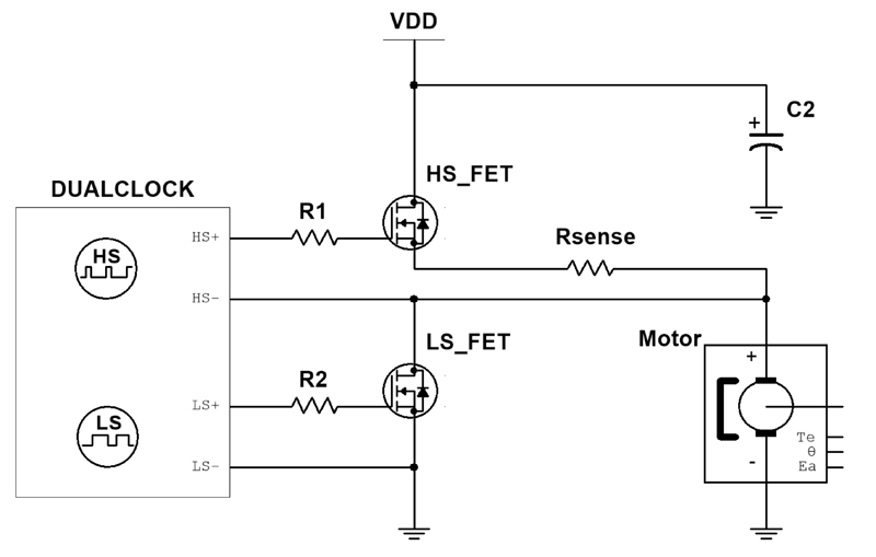
Click image to enlarge
Figure 1: Typical Application Circuit
The DUALCLOCK model has been simplified to run efficiently in SPICE, however, care should be taken to fully understand the threshold points and timing diagram. Study and understand the switching thresholds required for your application. For most simulation circuits, this will introduce only very small error terms in timing. The timing thresholds were selected at the extreme transition voltages (100% VGS) here for simplicity.
Figure 2 provides source code for the SPICE model. The high-side (HS) and low-side (LS) clocks are generated using two (Berkeley SPICE standard) independent voltage sources of type PULSE. Standard Parameters for Pulse include: Initial Voltage, Peak Voltage, Initial Time Delay, Rise Time, Falltime, Pulse Width, and Period of Wave. The pulse widths (TimeonHS and TimeonLS) are calculated as parameter lines for easier reading. The pulse width, as defined by Berkeley SPICE, is determined at maximum amplitude, which impacts the timing as mentioned previously.
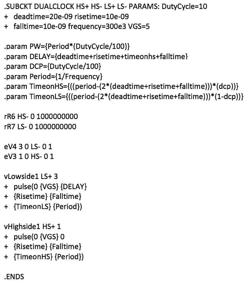
Click image to enlarge
Figure 2: DUALCLOCK SPICE Model
Actual implementation will require critical evaluation of the thresholds, but the modest impact on the duty cycle will not otherwise affect simulated analysis. By convention, this model keeps the high-side (HS) clock in-phase and the low-side (LS) clock out-of-phase. Duty cycle is generated with respect to the in-phase clock, and is consistent for use with Synchronous Rectification circuits, such as the Synchronous Buck Regulator. For example, 10% percent duty cycle would drive the low-side n-channel MOSFET on 90% of the time.
Some designers will attempt simulations utilizing two independent clock sources, adjusting each timing manually to avoid shoot-through. This process is tedious, error prone, difficult to synchronize correctly, and ultimately a flawed approach. Figure 3 shows the path that VDD current will follow while the High-side MOSFET is conducting.
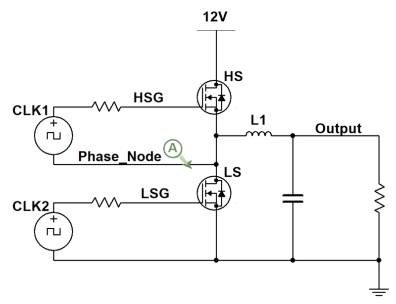
Click image to enlarge
Figure 3: Flawed Attempt at Solution
Your circuit will simulate, however, efficiency measurements and any thermal analysis will be grossly misrepresented. The switching cycle is typically small, so this error may go unnoticed. The two-terminal clock sources (CLK1 and CLK2) will sink current from the output inductor (L1), limited only by the gate resistor values selected. MOSFET HS will experience sharp temperature deltas during the conduction period. The DUALCLOCK model includes high-impedance inputs for both channels, limiting the current to realistic levels. Current to drive the clocks are sourced from the master simulation power supply as in the actual circuit, and will not be seen from the perspective of VDD.
The timing diagram of Figure 4 shows the relative timing of all edges. Both outputs are initially zero. Each cycle starts with the HS+ output at zero volts relative to the HS- pin of the model. HS+ output will rise to VGS volts above the HS- output. The rise time is set by model parameter Risetime. The differential output allows the HS- pin to be connected to voltages other than ground, normally the Phase node, which connects to the motor or output inductor of the power supply. HS+ output remains at VGS volts for the TimeonHS pulse-width interval.
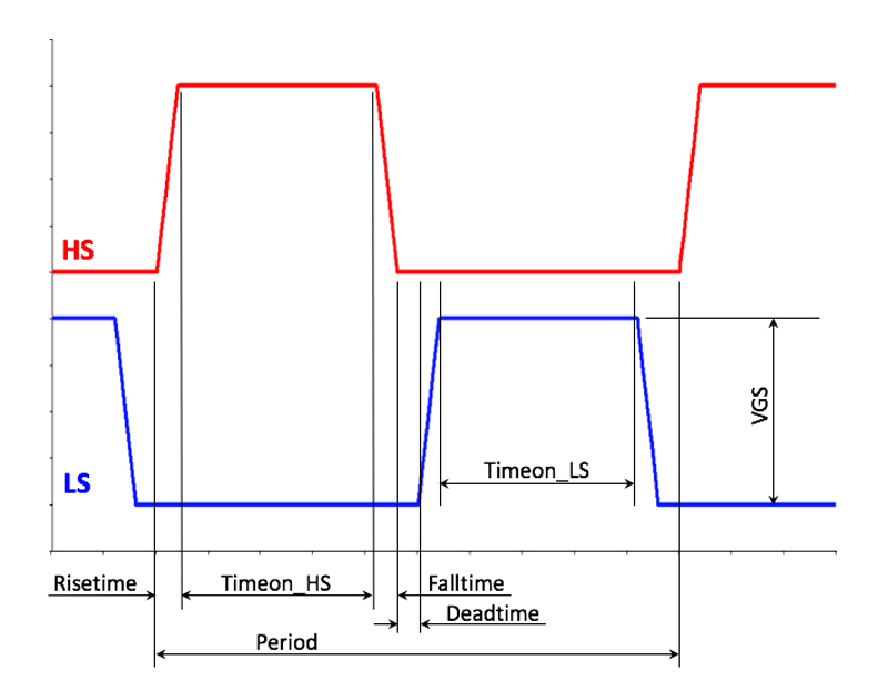
Click image to enlarge
Figure 4: Timing Diagram
The correct time is calculated by determining the period of the wave, subtracting the rise and fall times of both signals, subtracting the deadtime twice. Model parameter Dutycycle dictates the ratios between the high-side and low-side on times. HS+ output falls in accordance with the Falltime model parameter. Model parameter Deadtime delays the rising edge of the LS+ (low-side) output.
As above, there is a Risetime interval, followed by TimeonLS pulse-width interval, and finally a Falltime interval. One final Deadtime interval is inserted before the cycle concludes. HS- and LS- are internally pulled down through weak resistors, to provide single-ended outputs (HS+ and LS+) when left floating. This helps resolve convergence issues with most SPICE simulators.
The deadtime interval is critically important between the switching cycles as it eliminates possible shoot-through (a condition when both the high-side switch and the low-side switch are on simultaneously) in any full-bridge, half-bridge, PWM, Three-phase Brushless Motor, High-Current Transducer Drive, Switched Mode Power Supply, or other circuits that implement synchronous rectification. Slewrate control helps to reduce ringing and EMI issues, and also benefits Transient Analysis convergence by avoiding fast edges on the clocks. A later article will explain how to determine optimum deadtime.
DUALCLOCK model generates simulated voltage levels specified by model parameter VGS volts without limit. Thresholds for motors, control circuits, IGBT’s, or MOSFET’s will vary and are typically not the maximum value. Care must be taken when using slow slew rates, or long deadtimes, as this will impact the duty-cycle accuracy as specified by the DutyCycle model parameter. Negative deadtimes are allowed. While unrealistic, they are useful for analysis.
Please scrutinize your output waveforms from this model before driving critical components in your simulation. Read that sentence again. The peak value ratio (TimeonHS/TimeonLS) will equal the duty cycle, however, additional proportion of transition times will cause an error term. This is further complicated as the MOSFET gate-to-source voltage threshold (VGSth) varies with temperature. Model parameters are not checked for error conditions, so you can create discontinuous waveforms, or enter Deadtime values that exceed the period.
Figure 5 shows classic waveforms for the synchronous buck converter topology. These are graphed outputs from the Transient Analysis. Output inductor (L1) current rises during the high-side MOSFET TimeonHS interval, and falls during the low-side MOSFET TimeonLS interval. High-side gate-to-source voltage waveform shows typical ringing. The curves were scaled to fit the screen.
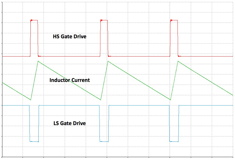
Click image to enlarge
Figure 5: Synchronous Buck Waveforms
Later articles will explore some useful test cases utilizing this model and others featured in the mini-series. Simulation results correlate well with actually laboratory testing. Procedures will be presented explaining test and simulation methods for identifying shoot-through conditions in synchronous buck designs. Keep simulating and have fun.