Using SPICE model blocks – Part Two

Clock-to-Gate driver SPICE Model
This article is Part Two of a mini-series, presenting useful SPICE model blocks to help motor control and power supply designers perform effective simulations. Part One introduced a block called “DUALCLOCK” that generates two floating clock outputs (see PSD, March 2017) for driving half-bridge circuits. The CLOCKDRIVER model presented here, converts one reference input clock to two, differential, out-of-phase clocks with programmable deadtime and slew-rate control. For power supply applications, such as true sinewave AC inverters, the designer will want to modulate the pulse width of the incoming clock (PWM signal). Of course, CLOCKDRIVER can also be utilized for driving half-bridge circuits, including traditional Synchronous Buck Converters, however, DUALCLOCK would be a simpler solution in that case with faster analysis times.
Circuits and application notes are readily available for DC-to-AC inverters (such as solar power converters), however, modeling these circuits is a different story. With the addition of proper building blocks, using traditional SPICE tools (such as Multisim by National Instruments)to simulate power supplies (converting or inverting) becomes much easier. For those of us that love to simulate, we know what a joy it is when a “block” or SPICE model is fully tested and available, ready to drop into our schematic so that we can continue to work on the circuit at hand, to solve and analyze our immediate needs. Without these tested blocks, we end up troubleshooting their models instead of our circuit. Presented here is another model that will converge cleanly, run quickly, and has been tested and proven.
CLOCKDRIVER can be utilized for finding optimum operating frequency of synchronous buck converters. Computer aided design using this block can help select or confirm values for the output stages. Simulating inverter waveforms takes a lot of computing horsepower, so please be patient with your simulation tools. High-frequency and low-frequency waveforms will both be present in the analysis. Slowing down the SLEWRATE will help your circuit converge and calculate quickly.
The typical application circuit is shown in Figure 1. This is a DC-to-AC power inverter application with simplified output stage. 200kHz Pulse Width Modulated (PWM) source is controlled by 60Hz voltage source. The output is a voltage, level controlled by the duty cycle of the clock input (CLK).
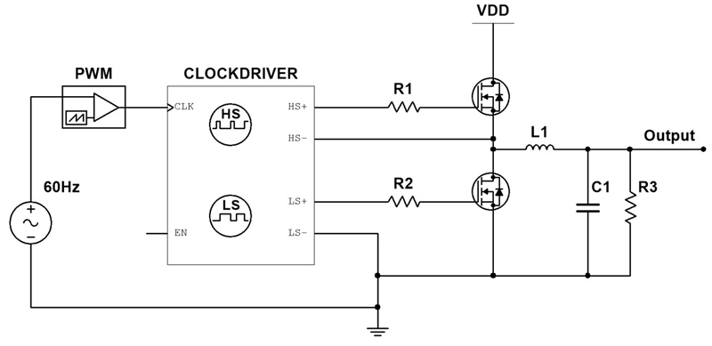
Click image to enlarge
Figure 1: Typical Application Circuit
CLOCKDRIVER creates two out-of-phase, differential, floating clock outputs, with programmable slewrate and deadtime, from a single-ended input clock. Duty cycle is controlled by the input clock. CLOCKDRIVER incorporates high-impedance buffers on the negative input terminals. Complementary differential outputs allow for floating connections, required for driving high-side MOSFET’s. Parameters utilized for each model instance specify SLEWRATE (risetime and falltime), DEADTIME (non-switching interval), and VGS (Gate-to-Source voltage). The CLOCKDRIVER model has been written to run efficiently in SPICE, however, care should be taken to fully understand the threshold points and timing diagram. There is a propagation delay of approximately 2.0ns through the block. External circuitry would be needed if the output must be synchronized with the input clock. Generally, this should not be a concern. Determine and understand the switching thresholds required for your application. There is also nominal duty cycle or phase distortion caused by SLEWRATE and DEADTIME variables. For most simulation circuits, this will introduce very small error terms in timing. Calculations internal to the model guarantee no shoot-through condition, since both outputs are held LOW before either signal switches HIGH. The clock input logic threshold is adjustable, but set internally to 2.5V. Output thresholds were selected at the extreme transition voltages (100% VGS) here for simplicity.
Figure 2 shows the schematic for CLOCKDRIVER, detailing the circuitry behind the model. The concept is simple, but following the SPICE syntax becomes quite complex rather quickly. Basically, the incoming clock (CLK) is split into in-phase and out-of-phase signals. The non-inverting buffer was added to the in-phase signal to maintain time integrity between the two clocks. Both signals are gated by the ENABLE input, which allows an application to cease switching both outputs. Output from the AND gates each pass through slew rate control and a gain block. These two blocks together with some simple algebra, ensure that the user inputs for slew rate and VGS are maintained for various conditions. Voltage-controlled-voltage-sources (V2 & V3) are included to add high-impedance inputs to the HS- and LS- inputs. By convention, this model keeps the high-side output (HS) in-phase and the low-side output (LS) out-of-phase with the reference clock input. Duty cycle is completely controlled by the input clock (CLK), consistent with Synchronous Rectification circuits, such as the Synchronous Buck Regulator. For example, 10% percent duty cycle for the input clock would drive the low-side n-channel MOSFET on 90% of the time. Figure 3 provides source code for the SPICE model. This model was written for National Instruments Multisim v14, and some functional block may require modification to use with other SPICE tools.
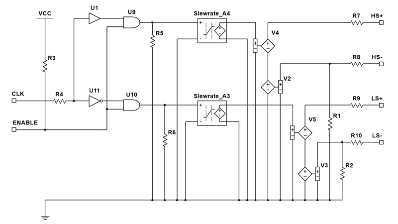
Click image to enlarge
Figure 2: Schematic for CLOCKDRIVER

Click image to enlarge
Figure 3: Source code for the SPICE model
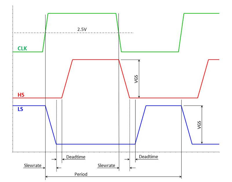
The timing diagram of Figure 4 shows the relative timing of all edges for the input clock (CLK) and the two outputs (HS & LS). Each cycle starts with the input clock (CLK) rising above the threshold voltage (set to 2.5V). LS output immediately starts to drop to zero, at the rate set by the SLEWRATE parameter. Both outputs remain low for the time interval set by the DEADTIME parameter. HS+ output will begin to rise VGS volts above the HS- terminal, at a rate set by the SLEWRATE parameter. Both outputs will remain unchanged until the input clock (CLK) drops below the threshold voltage (set to 2.5V). The HS output will drop immediately at the rate set by SLEWRATE, and pause for the interval set by DEADTIME. LS will then rise at the rate set by SLEWRATE. The cycle completes when LS begins to drops again.
Click image to enlarge
Figure 4: Relative timing of all edges for the input clock (CLK) and the two outputs (HS & LS)
The differential output pairs, HS+/HS- and LS+/LS-, will generate relative voltage swings set by the VGS parameter. This differential output scheme allows the HS- pin to be connected to voltages other than ground, normally the Phase node, which connects to the motor or output inductor of the power supply. LS- may be connected to a reference node, such as a sense resistor, or connected directly to ground. Gate drive circuitry will drive the VGS signal as intended, creating a differential level fro Gate-to-Source. HS- and LS- are internally pulled down through weak resistors, to provide single-ended outputs (for HS+ and LS+) when left floating, which is helpful for testing and waveform analysis. Additional resistors located inside the model further help resolve convergence issues with most SPICE simulators. The Enable pin is internally pulled-up, and may be left floating if unused.
The deadtime interval is critically important between the switching cycles, as it eliminates possible shoot-through conditions, (when both MOSFETs are conducting simultaneously) in any full-bridge, half-bridge, PWM, Three-phase Brushless Motor, High-Current Transducer Drive, Switched Mode Power Supply, or other circuits that implement synchronous rectification. To improve duty cycle accuracy, your input clock should have fast edges relative to the SLEWRATE parameter. Slewrate control helps to reduce ringing and EMI issues, and also benefits Transient Analysis convergence problems by avoiding fast edges on the clocks. A later article will explain how to determine optimum deadtime.
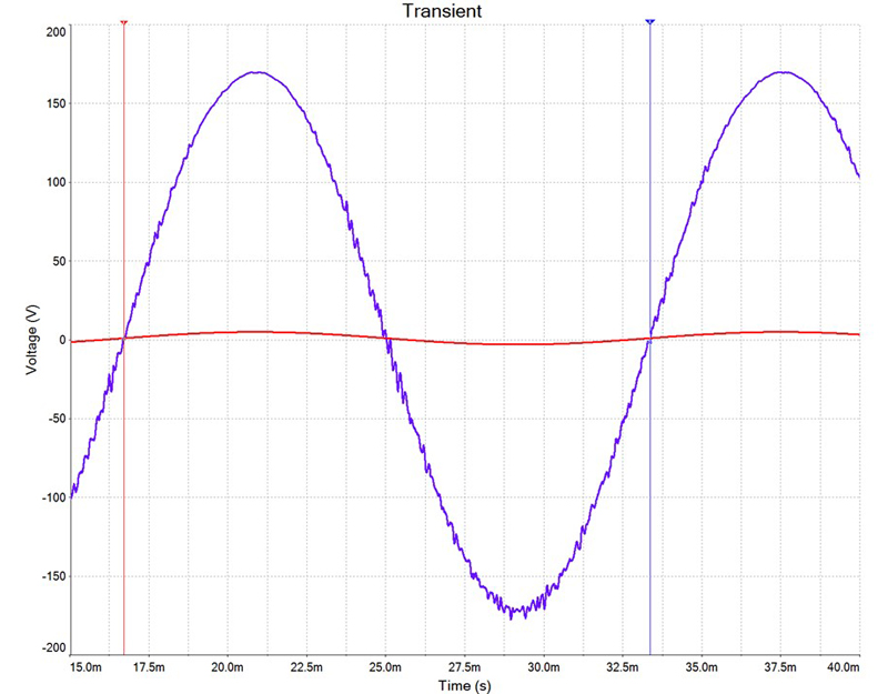
Figure 5 shows the output of the DC-to-AC inverter simulation Transient Analysis, with 120VAC output waveform displayed compared with the reference 60Hz modulating sine wave. This output could easily be sent through a transformer and filter stage to remove the high-frequency noise. Analyzing power supply circuits with SPICE is never simple. Expect convergence errors and long analysis times that never seem to end. My friend, Jason Foster, had requested that this model be created and helped with troubleshooting. I am grateful for his friendship and his assistance. Keep in mind, that just like circuits, the analysis is performing EXACTLY the task that you requested, but possible not the task that you had intended. Results are mathematical calculations. Nothing more. The circuit is not real, it is just an illusion. Read that sentence again. Strange inputs will yield strange results.
Click image to enlarge
Figure 5: Output of the DC-to-AC inverter simulation Transient Analysis, with 120VAC output waveform displayed compared with the reference 60Hz modulating sine wave
Later articles will explore some useful test cases utilizing this model and others featured in the mini-series. Simulation results correlated very well with actually laboratory testing. Procedures will later be presented explaining test and simulation methods for identifying shoot-through conditions in synchronous buck designs. Keep simulating and always have fun.