An overview of Infineon’s SiC MOSFETs and dedicated gate driver ICs
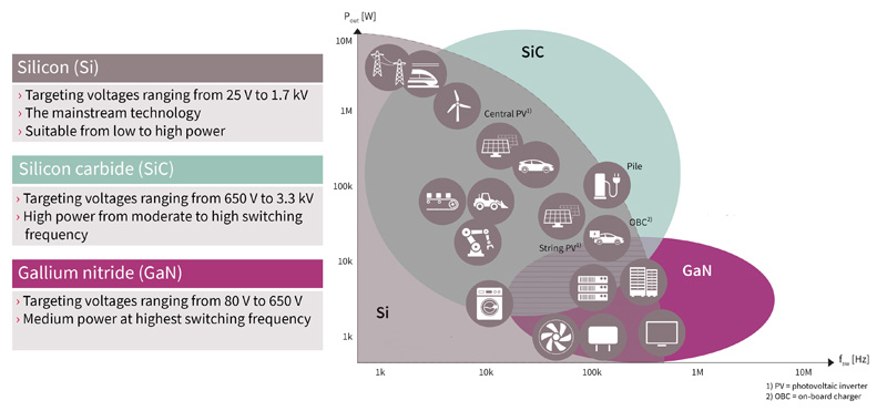
Figure 1 Technology positioning – Si, SiC and GaN
The global trends - such as digitalization and energy efficiency - that have emerged and accelerated in the past few years pose new challenges to the manufacturers as well as the semiconductor market. Developing power semiconductor devices that contribute to highly efficient power management systems is on the agenda for all of the players in the industry.
Power semiconductors as the building blocks of power systems are among the very determinant contributors to energy efficiency. Designers of power systems - from power supplies to inverters - are required to fulfill progressively challenging efficiency targets while also keeping costs under control. The cost factor plays an important role over and beyond making the bottom line of OEMs rosier. If solar inverters, high-efficiency power supplies, and electrical vehicles become cheaper, that will foster the adoption of greener infrastructure and have a positive effect on the future of our planet and hence also humankind.
The technology of choice
From a designer’s perspective, a reasonable and balanced combination of cost and efficiency is essential. In addition to the legacy silicon, recently new technologies and materials - such as silicon carbide (SiC) and gallium nitride (GaN) - have emerged with the promise of delivering higher efficiency and power density levels. Indeed, WBG semiconductors have - by the nature of the materials - a great potential to deliver pioneering performance. They enable higher breakdown voltages, higher frequency operations, more flexible thermal capability, and robustness to hard-commutation events. All these characteristics make them better-suited for new high-efficiency topologies or high-density designs than Si-based solutions.
Where is the sweet spot for each power technology?
As shown in Figure 1, Si-based products like superjunction MOSFETs or IGBTs can be used over a wide voltage range (from a few to several hundred volts) and in several power classes while SiC-based products find their ideal spot in voltage classes at and above 650 V (pushing beyond silicon limits and reaching power levels above 3 kV), and GaN-based devices are more suitable for voltage classes below 650 V. Both SiC and GaN are progressively better than Si when the operating frequency increases. Application requirements and design targets determine the technology of choice.
Looking at the three technologies and focusing on discrete FET products only, Infineon has a broad portfolio in the 600 - 650 V range (CoolMOS™ silicon superjunction MOSFETs, CoolSiC™ silicon carbide MOSFETs, and CoolGaN™ gallium nitride normally-off e-mode HEMTs). Although SJ MOSFETs fulfill most of the contemporary requirements for energy efficiency and power density in a very cost-optimized way, in case of some specific design requirements such as thermals or ultra high density SiC and GaN devices are the optimal choice. The CoolSiC™ MOSFETs demonstrate superior thermal properties thanks to their device ruggedness and CoolGaN™ HEMTs are suitable for high operating frequencies pushing the power density to very high levels.
In the future, WBG products are expected to further accelerate and replace silicon-based devices, however, these three technologies will foreseeingly still coexist for long time. The adoption of SiC is expected to be a bit faster for certain applications due to its ease of use and relatively easy transition from superjunction MOSFETs and IGBTs.
Infineon’s CoolSiC™ MOSFETs were developed to perform
SiC technology when used in the right design approach is the best choice for applications that require high-performance.
Click image to enlarge
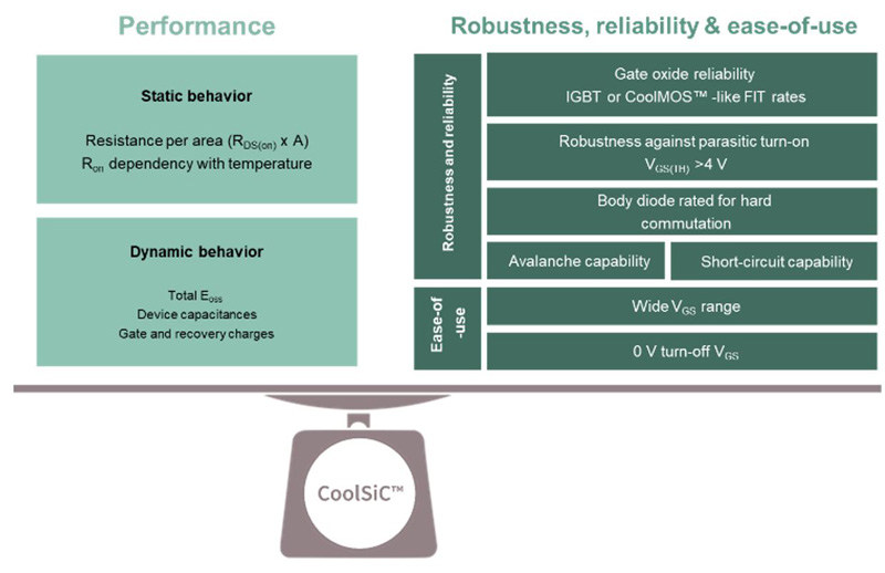
Figure 2 The features and characteristics of Infineon’s CoolSiC™ MOSFET 650 V devices at a glance
However, the area-specific on-state resistance is the major benchmark parameter for a given technology, it is still essential to find the right balance between the primary performance indicators (i.e., resistance and switching losses) and the true operating behavior. The CoolSiC™ MOSFETs and the matching EiceDRIVER™ gate drivers were developed to fully leverage the promise of SiC: deliver performance through robustness, reliability, and ease-of-use. For the available portfolio see Figure 2.
Click image to enlarge
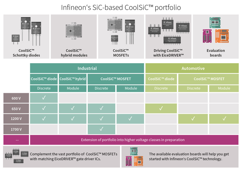
Figure 3 Infineon’s SiC-based CoolSiC™ portfolio
When it comes to reliability, SiC MOSFETs have a key potential failure point in the gate oxide (GOX), the layer which insulates the gate from the source. SiC crystal growth tends to inject defects into the structure and those defects that penetrate the GOX can create local thinning, ultimately increasing the electrical field beyond the dielectric breakdown and eventually destroying the device. To avoid this, the CoolSiC™ MOSFETs are based on a trench structure which provides two major benefits:
· fewer defects in the GOX, due to the orientation of the structure
· increased GOX thickness with no compromises on performance (a thicker GOX can be chosen with no impact on Ron) thanks to increased robustness and higher achievable electrical field intensity (which allows for testing at higher voltages, increasing the effectiveness of the defect-screening)
When it comes to performance, the CoolSiC™ MOSFETs are characterized by very low switching- and conduction losses improved by a relatively flat dependency of the RDS(on) with temperature. In particular, the robustness against parasitic turn-on has not only a positive effect on the switching losses but is also significant in terms of ease-of-use. Thanks to the low tendency to parasitic turn-on behavior, the CoolSiC™ MOSFETs are the only devices in the market that can authentically be switched off at 0 V, without the need of using negative voltages (although the device can be used that way too). Resultantly, the driving schema can be kept simple and is fully compatible with superjunction MOSFET driving solutions.
With regards to the driving voltage range, some voltage margin between the upper limit of the VGS range and the maximum tolerated voltage (VGS,max; specified in the datasheet) is needed. This margin guarantees the buffer to protect against the overshoots that may stress and damage the gate oxide. This is an additional token that the CoolSiC™ technology pays to reliability.
EiceDRIVER™ ICs make the solution complete
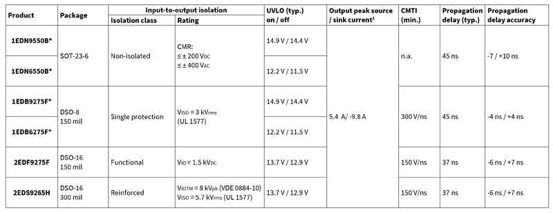
Six dedicated gate driver ICs have been developed in order to optimally drive and protect Infineon’s CoolSiC™MOSFET 650 V devices. As shown in Figure 4, they are available in four differentpackages to allow an easy adaptation to different design requirements in terms of power density, PCB space, and isolation rating [1].
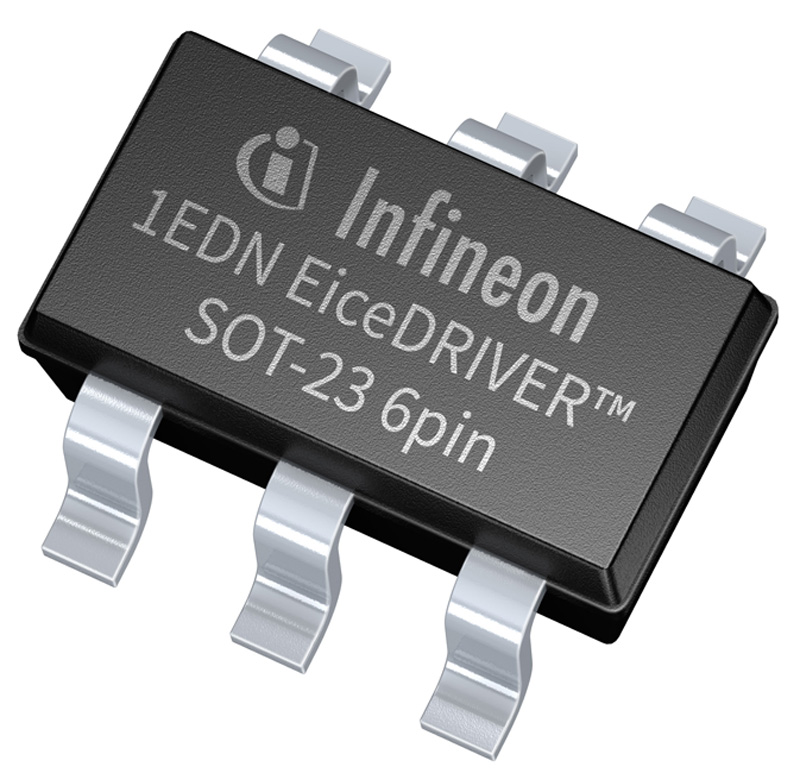
The single-channel non-isolated EiceDRIVER™ ICs 1EDN9550B and 1EDN6550B are available in the SOT-23 6-pin package and can be used to drive the low-side switch of a SiC half-bridge (HB) [2]. Due to their truly differential inputs (TDI) they are particularly well suited to drive 4-pin MOSFETs with Kelvin-source connection. The unique differential driving concept can safely prevent false triggering due to resistive or inductive voltage drops between controller and driver IC reference potentials even for very fast switching transients [3]. As a result, the TDI gate driver ICs provide a compact and robust solution for the highly efficient operation of SiC MOSFETs.
The isolated EiceDRIVER™ ICs 1EDB9275F and 1EDB6275F are offered in a DSO-8 150mil package, featuring 3 kVrms isolation voltage rating according to UL 1577 (certification pending) [4]. In combination with the TDI driver, a hybrid gate driving configuration can be obtained to drive SiC HB in totem-pole PFC or resonant LLC topologies.The increased layout flexibility, obtained by employing single-channel gate driver ICs,allows optimizing the driver IC placement on the PCB in order to minimize the gate loop parasitic inductances. Furthermore, this hybrid gate driving configuration results in a 28% PCB area saving (compared with a dual-channel gate driver IC) and it comes with a competitive bill of materials (BOM).
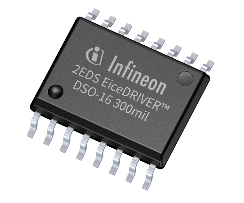
The alternative gate driving solutions are enabled by utilizing Infineon’s dedicated dual-channel isolated gate driver ICs. The EiceDRIVER™ 2EDF9275F, available in a DSO-16 150mil package, is a perfect fit for the totem-pole PFC topology [5]. And if the PWM signals have to cross the safe isolation barrier, such as in the resonant LLC with secondary-side control, the 2EDS9265H with reinforced isolation is the right choice. Furthermore, this driver comes in a DSO-16 300mil package and is compliant with the safety requirements of the VDE 0884-10 and UL 1577 standards [6].
Click image to enlarge
Figure 4a: 1EDN9550B, 1EDN6550B, SOT-23 6-pin

Click image to enlarge
Figure 4b: 1EDB9275F, 1EDB6275F, DSO-8 150mil

Click image to enlarge
Figure 4c: 2EDF9275F, DSO-16 150mil
Click image to enlarge
Figure 4d: 2EDS9265H, DSO-16 300mil
Table 1 shows the main specifications of the dedicated gate driver ICs for Infineon’s CoolSiC™ MOSFET 650 V devices. Despite the different packages and input-to-output isolation classes, ratings, and certifications, these gate drivers are based on the same rail-to-rail driver output stage. It is realized with complementary MOS transistors that can provide a typical 5.4 A sourcing and 9.8 A sinking current for fast turn-on and turn-off to minimize switching losses. With an RON of 0.85 Ω for the sourcing pMOS and 0.35 Ω for the sinking nMOS transistor, the driver can be considered as a nearly ideal switch, enabling it to run cooler due to less power dissipation in the IC.
The common-mode transient immunity (CMTI) is crucial to ensure that no signal corruption occurs during fast transients applied between the input and output reference potentials (grounds) of the galvanically isolated gate driver IC. Since SiC MOSFETs can generate fast voltage transients exceeding 100 V/ns, CMTI is a key parameter to be considered for gate driver selection. 1EDB6275F and 1EDB9275F ensure a minimum 300 V/ns CMTI robustness, while the 2EDF9275F and 2EDS9265H feature a minimum 150 V/ns, which by far exceeds the requirements for the majority of fast-switching SiC applications.
The timing performance of the driver is also of particular importance in order to exploit the full potential of SiC MOSFETs. The low input-to-output propagation delay combined with high accuracy over both temperature and production variations allows for using a short dead-time period between the two PWM signals of the half-bridge; this improves efficiency by increasing the effective power transfer period.
Click image to enlarge
Table 1 Gate driver ICs for Infineon’s CoolSiC™ MOSFETs 650 V
* Coming soon; 1VDDO = 15 V, VOUT = 0 V, Tamb = 25°C
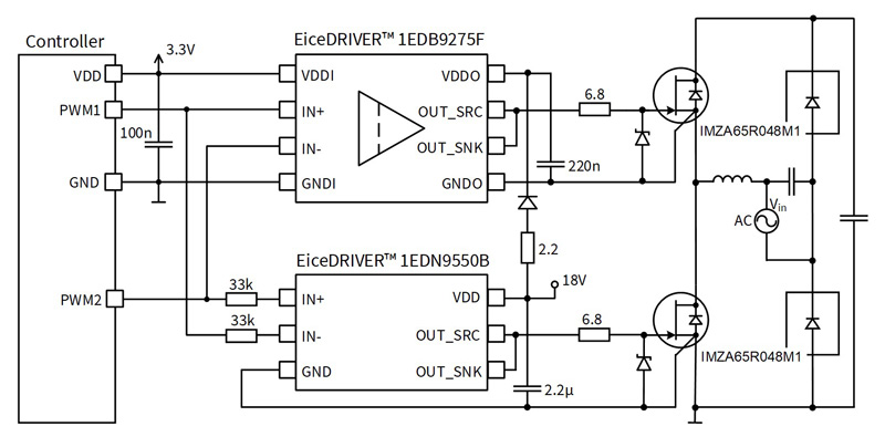
Figure 5 depicts a typical use case for Infineon’s CoolSiC™ MOSFETs 650 V in a totem-pole PFC. It consists of a 48 mΩ SiC half-bridge driven by the EiceDRIVER™ 1EDB9275F and 1EDN9550B in the hybrid gate driving configuration; the diode functions indicated in the power path are usually realized with low-RDS(on) MOSFETs operating as synchronous rectifiers. As a result, this power stage can handle up to 3.3 kW with an efficiency above 99% [7].
One of the benefits of Infineon’s wide-bandgap (WBG) technology is the possibility of using standard gate drivers, since driving voltages of 0 V and 18 V, respectively, are recommended. As demonstrated in [8], an 18 V gate drive voltage reduces the RDS(on) by around 18% compared with a 15 V drive. Anyway, considering the portfolio listed in Table 1, the customer has plenty of options in terms of under-voltage lockout (UVLO) levels to choose the best-suited gate drive voltage. The UVLO feature ensures that in case the output-side supply voltage VDDO drops to a level that would cause the power switch to operate in its linear mode, the gate driver IC will keep the transistor “off” and within its safe operating area (SOA), thereby avoiding any excessive power dissipation. With a typical UVLOoff of 11.5 V, 1EDN6550B and 1EDB6275F are the right choice for 15 V gate driving. For applications with a higher gate driving voltage (e.g., 18 V), 1EDN9550B, 1EDB9275F, 2EDF9275F, or 2EDS9265H have to be selected since they feature a higher UVLOoff level. Additionally, and as represented in Figure 5, it is recommended to connect a Schottky diode between gate and Kelvin-source to clamp switching induced undershoots on the gate terminal which may cause a potential drift of the gate threshold voltage VGS(th) over the lifetime.
Since the 1EDB9275F, 1EDB6275F, 1EDN9550B and 1EDN9550B and 1EDN6550B have inverting (IN-) and non-inverting (IN+) inputs, shoot-through protection can be implemented by routing both PWM signals to each gate driver IC, as depicted in Figure 5; any undesired overlap of low-side and high-side PWM signals is not propagated to the gate of the transistors. In case this additional protection feature is not required, it can simply be disabled by connecting IN- to GNDI.
To summarize, the 1-channel and 2-channel galvanically isolated gate-driver ICs of the EiceDRIVER™ family are the best choice to operate Infineon’s CoolSiC™ MOSFET 650 V devices to achieve the optimum combination of efficiency, power density, and robustness in high-performance power conversion applications.
Click image to enlarge
Figure 5 Hybrid gate driving of the CoolSiC™ MOSFET 650 V based on the EiceDRIVER™ 1EDB9275F and 1EDN9550B
References:
[1]D. Varajao and C. M. Matrisciano, “Isolated gate driving solutions: increasing power density and robustness with isolated gate driver ICs,” Infineon Technologies AG, Application Note AN_1909_PL52_1910_201256, 2020
[2]Infineon Technologies AG, “EiceDRIVER™ 1EDN-TDI low-side gate drivers with Truly Differential Inputs (TDI),” 2019. [Online]. Available: https://www.infineon.com/1edn-tdi
[3] Infineon Technologies AG, “Applications of 1EDNx550 single-channel low-side EiceDRIVER™ with truly differential inputs,” Application Note AN_1803_PL52_1804_112257, 2018
[4] Infineon Technologies AG, “EiceDRIVER™ 1EDB single-channel isolated gate driver,” 2020. [Online]. Available: https://www.infineon.com/1edb
[5]Infineon Technologies AG, “EiceDRIVER™ 2EDi dual-channel isolated gate driver,” 2018. [Online]. Available: https://www.infineon.com/2edi
[6]Infineon Technologies AG, “Using the EiceDRIVER™ 2EDi product family of dual-channel functional and reinforced isolated MOSFET gate drivers,” AN_1805_PL52_1806_095202, 2019
[7]Infineon Technologies AG, “3300 W CCM bi-directional totem pole with 650 V CoolSiC™ and XMC™,” Application Note AN_1911_PL52_1912_141352, 2020
[8]Infineon Technologies AG, “CoolSiC™ MOSFET 650 V M1 trench power device: Infineon’s first 650 V silicon carbide MOSFET for industrial applications,” Application Note AN_1907_PL52_1911_144109, 2020