Many consumers are gaining interest in ways to monitor and maintain their good health
The pervasiveness of diabetes and obesity, as well as high cholesterol levels due to changes in lifestyle, in conjunction with the proliferation of smartphones and wearable devices, are influencing consumers to adopt various health monitoring applications to assist them to maintain their optimal health.
Accordingly, patient centric healthcare applications are helping users to stay updated about medication times, number of calories consumed, dehydration levels in body and so forth, A common way or doing this is via a mobile-like phone. By way of example, Apple Inc., released a statistic where they stated that on an average, an iPhone user unlocks their phone 80 times a day. This makes it an ideal methodology in which to receive and view biometric data. This creates a large target population for developers of health applications, as well as, the hardware platform manufactures of portable health monitoring products to sell their wares.
This increasing trend towards healthcare information technology systems enables access to patients’ data to practitioners sitting anywhere in the world. And that’s not all, routine checkup of lab reports as well as easy access to radiology and pathology reports from mobile devices will no doubt boost the growth of patient centric healthcare applications. Figure 1 shows an example of a typical monitoring system once it has been placed onto a user.
Medical Devices
Analog Devices Inc. has serviced the medical market segment for many decades. Accordingly, we have observed that low power precision components have enabled the rapid growth of portable and wireless medical devices. Nevertheless, these types of medical products generally have a high standard for reliability, run-time and robustness. Accordingly, much of this burden falls on the power management system and its components. Medical monitoring products must operate properly and switch seamlessly between a variety of power sources such a battery, an AC mains outlet, supercapacitors and even harvested ambient energy sources.
It should be obvious that the power systems architect needs to go to great lengths to protect against, and tolerate fault conditions, maximize operating runtime (if powered from batteries); while also ensuring that normal system operation is reliable whenever a valid power source is present.
Another current key trend fueling the growth of portable and wireless medical instrumentation is patient care. Specifically, this can be attributed to the increased use of remote monitoring systems within a patient’s own home. The reason for this trend is purely economic in nature – the costs of keeping a patient in a hospital are becoming prohibitive – both for the patient and the medical provider. This accounts for the growing trend to have many of these portable electronic monitoring systems incorporate radio frequency (RF) transmitters so that any data gathered from the patient can be sent directly back to a supervisory system within the hospital or doctor’s office, for later review and analysis.
Given the above scenario, it is reasonable to assume that the cost of supplying the appropriate medical instrumentation to the patient for home use is more than offset by the cost of keeping them in the hospital for observation purposes. Nevertheless, it is of paramount importance that the equipment used by the patient be reliable and fool-proof. As a result, the manufactures and designers of these products must ensure that they can run seamlessly from multiple power sources and have high reliability in their wireless data transmission of the data collected from the patient. This requires the power management and conversion architecture to be robust, flexible, compact, efficient and low noise over a wide bandwidth.
Power Conversion Architecture
Although switching regulators generate more noise than linear regulators, their efficiency is far superior. Noise and EMI levels have proven to be manageable in many noise sensitive applications if the switcher behaves predictably. If a switching regulator switches at a constant frequency in normal mode, and the switching edges are clean and predictable with no overshoot or high frequency ringing, then EMI is minimized. A small package size and high operating frequency can provide a small tight layout, which also minimizes EMI radiation. Furthermore, if the regulator can be used with low ESR ceramic capacitors, both input and output voltage ripple can be minimized, which are additional sources of noise in the system. Nevertheless, not all system architects have a comprehensive switch mode power conversion background to address these noise interference aspects.
Furthermore, many of these systems require 1.xV, 2.xV or 3.xV rails for powering low power sensors, memory, microcontroller cores, I/O and logic circuitry. Moreover, to complicate matters even further for the power systems architect, there are usually thermal design constraints in their systems due to their virtual lack of no air flow or heat-sinking in the end equipment for cooling purposes.
Accordingly, Analog Devices’ Power by Linear product group hasfocused on bringing solutions to these problems with its own high levels of product innovation and expertise. For example, there are many applications in medical electronic systems that require continuous power even when the mains supply is interrupted, such that a back-up power system is usually necessary. The back-up run time of these systems is generally defined by the time the system needs to shutdown properly after its main supply is lost. This time will vary depending on the end application from minutes to hours. And to complicate matters further, the number of power rails in these feature-rich medical devices continues to increase while their operating voltages continued to decrease.
New Solutions to Ease Design Constraints
Supercapacitors are an excellent choice for systems that need high power, short duration backup power. Accordingly, any IC that supports this type of application would typically require the capability to support 2.9 V to 5.5 V supply rails during a main power interruption. It is well known that supercapacitors have high peak power capabilities, making them an ideal choice for systems whose applications require high peak power backup for brief time intervals. By way of example, the LTC4041 from PbL uses an on-chip bidirectional synchronous converter to provide high efficiency step-down supercapacitor charging, as well as high current, high efficiency boost backup power. When external power is available, the device operates as a step-down charger for one or two supercapacitor cells while giving preference to the system load. When the input supply drops below the adjustable power fail indicator (PFI) threshold, the LTC4041 switches to step-up mode operation and can deliver up to 2.5 A to the system load from the supercapacitor(s). During a power fail event, the device’s PowerPath control provides reverse blocking and a seamless switchover from input power to backup power. Typical applications for the LTC4041 include ride-through “dying gasp” supplies like those typically found in medical equipment, power meters, industrial alarms and solid-state drives. Figure 1 shows a typical LTC4041 application schematic.

Click image to enlarge
Figure 1. LTC4041 single supercapacitor backup for 3.3V system.
If two supercapacitors are used, an internal supercapacitor balancing circuit maintains equal voltages across each supercapacitor and limits the maximum voltage of each supercapacitor to a predetermined value. Its adjustable input current limit function enables operation from a current limited source while prioritizing system load current over battery charge current. An external disconnect switch isolates the primary input supply from the system during backup. The device also includes input current monitoring, an input power fail indicator, and a system power fail indicator. The LTC4041 also includes an optional OVP function using an external Mosfet that can protect the IC from input voltages greater than 60V.
Moreover, for power supply designers of thermally and space constrained medical systems, is the recent introduction of a product which address the need for a small, compact and efficient 5V buck converter that has high conversion efficiency to minimize thermal constraints and also has a very small solution footprint and height profile.
Accordingly, the PbL product group recently introduced the LTC3309A to specifically address space and thermal design constraints. The LTC3309A is a very small, low noise, monolithic step-down DC/DC converter capable of providing up to 6A of output current from a 2.25V to 5.5V input supply. The part employs Silent Switcher® architecture with external hot loop bypass capacitors to achieve both low EMI and high efficiency at switching frequencies as high as 3MHz. Moreover, the LTC3309A is a constant frequency, current mode step-down DC/DC converter. An oscillator turns on the internal top power switch at the beginning of each clock cycle. Current in the inductor increases until the top switch current comparator trips and turns off the top power switch. The peak inductor current at which the top switch turns off is controlled by the voltage on the ITH node. The error amplifier servos the ITH node by comparing the voltage on the FB pin with an internal 500mV reference. When the load current increases, it causes a reduction in the feedback voltage relative to the reference leading the error amplifier to raise the ITH voltage until the average inductor current matches the new load current. When the top power switch turns off, the synchronous power switch turns on until the next clock cycle begins or, in pulse-skipping mode, inductor current falls to zero. If overload conditions result in excessive current flowing through the bottom switch, the next clock cycle will be delayed until switch current returns to a safe level. If the EN pin is low, the LTC3309A is shut down and in a low quiescent current state. When the EN pin is above its threshold, the switching regulator will be enabled.
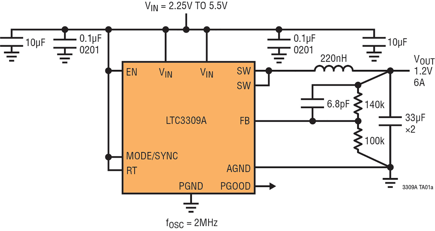
Click image to enlarge
Figure 2. LTC3309A application schematic delivering 6A at 1.2V from a 2.25V to 5V input
Since the LTC3309A uses a constant frequency, peak current mode control architecture it can provide fast transient response with minimal output capacitance. A 500mV reference allows for low voltage outputs, while 100% duty cycle operation delivers low drop out. Other features include a power good signal when the output is in regulation, precision enable threshold, output overvoltage protection, thermal shutdown, a temperature monitor, clock synchronization, mode selection and output short circuit protection. The device is available in a compact 12-lead 2mm x 2mm LQFN package.
Conclusion
There can be no doubt that the system designers of portable and wireless medical monitoring devices used for in-home patient health monitoring purposes face daunting design challenges. These include the coalescence of constraints that they must accommodate; many of which seem to be mutually exclusive. Examples are both space and thermally constrained enclosures, as well as being able to transmit data without interference or interruption. Fortunately, thanks to Analog Devices’ PbL group, the recent product introductions of the LTC3309 and LTC4041, the designer has viable solutions to meet the demands for small, compact and thermally efficient solutions that will fit into equipment form factors.
Analog Devices