Where do I connect the grounds of switching regulators?
How should you proceed with a switching regulator with an analog ground (AGND) and a power ground (PGND)? This is a question asked by many developers designing a switching power supply. Some developers are accustomed to dealing with a digital GND and an analog GND; however, their experience frequently fails them when it comes to the power GND. Designers then often copy the board layout for a selected switching regulator and stop thinking about the problem.
PGND is the ground connection over which higher pulsed currents flow. Depending on the switching regulator topology, this means the currents through a power transistor or the pulsed currents of a power driver stage. This is especially relevant in the case of switching controllers,forexample, with external power switches.
AGND, sometimes called SGND (signal ground), is the ground connection that the other, usually very calm, signals use as a reference. This includes the internal voltage reference needed for the regulation of the output voltage. Soft start and enable voltages are also referenced to the AGND connection.
There are two different technical philosophies, and thus different opinions among experts regarding the handling of these two ground connections.
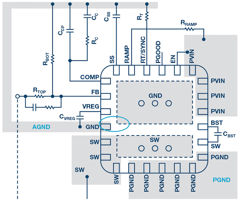
According to one philosophy, the AGND and PGND connections on a switching regulator IC should be joined to each other right next to the respective pins. This keeps the voltage offset between the two pins relatively low. Thus, the switching regulator IC can be protected from disturbances and even destruction. All of the circuit’s ground connections and a possible ground plane would be linked to this common point in a star topology. Figure1 shows an example implementing this philosophy. The board layout for an LTM4600 is shown here. It is a 10 A step-down micromodule. The separate ground connections on the board are joined right next to each other (see the blue oval in Figure 1). Due to the parasitic inductance of the respective bonding wires between silicon and the housing, as well as the inductances of the respective pins, there is already a certain amount of decoupling of PGND and AGND, resulting in a low amount of mutual interference between the circuits on the silicon.
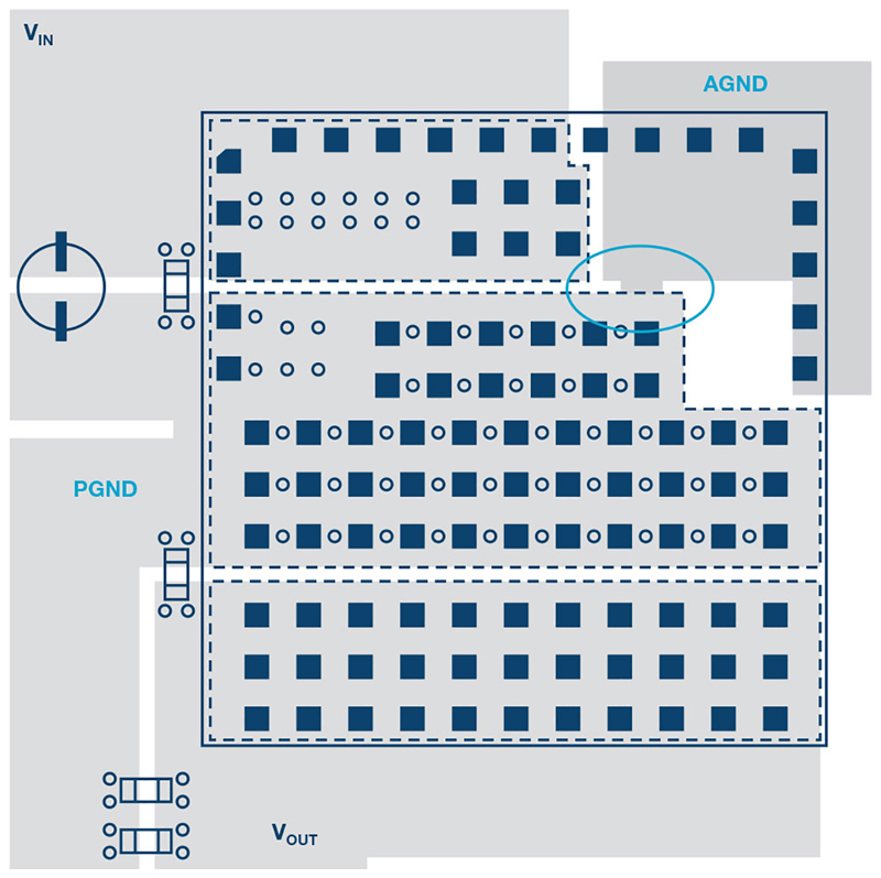
Click image to enlarge
Figure 1. Local connection of PGND and AGND right at the solder contacts
The other philosophy involves additional separation of AGND and PGND on the board into two separate ground planes connected to each other at one point. Through this connection, interfering signals (voltage offset) remain largely in the PGND region, while the voltage in the AGND region remains very calm and decoupled very well from PGND.However, the disadvantage is that, depending on the transients in the pulsed currents and the current intensities, there may be a significant voltage offset between PGND and AGND at the respective pins. This can lead to improper functioning of, or even damage to, a switching regulator IC. Figure 2 shows an implementation of this philosophy. This comes from an ADP2386, a 6 A step-down switchingregulator.
Click image to enlarge
Figure 2. Separated AGND and PGND connected under the GND tab by vias
The grounding question comes down to a trade-off between strong separation with the advantage of separating noise and disturbances and running the risk of generating voltage offsets between the two grounds and thus causing harm to silicon and compromising functionality. The right decision to make in regard to this trade-off is heavily based on the IC design, including switching transition speeds, power levels, parasitic inductances on bonding wires and IC package, and the latch-up risk of each IC design involving the individual semiconductor process.
The answer to the question of how to deal with the grounds AGND and PGND is not that simple.That’s why this discussion continues. A the beginning, I mentioned that many users of switching regulators adopt the board layout and the ground connection type from the example circuit supplied by the IC manufacturer. This procedure is useful because you can usually assume that the manufacturer also tested the respective IC in this configuration. It can also be seen in the examples given in Figure 1 and Figure 2 that there spective IC pinout is suitable for local ground connection close to PGND and AGND, or for separate grounding.
Of course, an IC manufacturer may make mistakes when designing example circuits. That’s why it’s good to have some further information about the underlying philosophies.