Why GaN Enables High Efficiency in Totem-Pole PFC-Based Power Designs
Modern-day trends such as electric vehicles, cloud computing, blockchain mining and 5G telecommunications have greatly increased the power consumed in our daily lives.
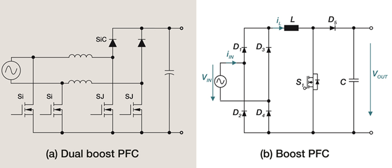
Figure 1: PFC topologies: dual-boost PFC (a) and boost PFC (b)
Almost all of the popular modern-day trends involve an AC/DC power supply, which takes energy from the AC grid and delivers it to the electrical equipment as a well-regulated DC. With the increasing power consumption in these systems, the associated energy losses in the AC/DC power conversion process becomes a significant component of the overall cost equation. Reducing losses in the AC/DC power supply can help lower the cost of ownership of the end application.
Government regulations worldwide mandate the use of a power factor corrector (PFC) stage in the AC/DC supply in order to facilitate a clean power draw from the grid. A PFC shapes the AC input current to follow the same shape as the AC input voltage, which maximizes the real power drawn from the grid, making the electrical equipment act like a pure resistor with zero reactive power. Without a PFC stage, the grid consumes the reactive power from the electrical equipment, which translates into higher costs for consumers, since power companies have to generate more power for transmission and distribution. Adding PFCs in power converters can save energy generated by power companies by introducing a switching stage that reduces losses.
By enabling a 0.8% efficiency gain, a gallium nitride (GaN)-based totem-pole PFC can enable a 100-MW data center to save as much as $7 million in energy costs over a period of 10 years. This is an example of why there is a worldwide market push to design very efficient PFCs that can help reduce energy losses in power converters. A PFC stage is typically found in electrical equipment power supplies for servers; telecommunication rectifiers; blockchain mining; onboard chargers; heating, ventilation and air conditioning units; and battery test systems.
PFC stage topologies
As shown in Figure 1, traditional PFC topologies include the boost PFC (with a full-bridge rectifier after the AC line) and dual-boost PFC. The classical boost PFC is a common topology that contains a front-end bridge rectifier that has very high conduction losses. The dual-boost PFC reduces conductions losses since it does not have that front-end bridge rectifier, but it needs an additional inductor and hence suffers in terms of cost and power density.
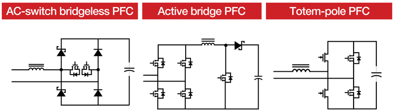
Other topologies that may increase efficiency include AC-switch bridgeless PFC, active-bridge PFC and bridgeless totem-pole PFC, shown in Figure 2. The AC switch topology has two high-frequency FETs conducting during the on-state and one silicon carbide (SiC) diode plus a silicon diode conducting during the off-state. Active-bridge PFC simply replaces the diode bridge rectifier connected to the AC line with four low-frequency FETs, which require additional control and driver circuitry. Active-bridge PFC uses three FETs (two low- frequency FETs and one high frequency FET) conducting during the on-state and two low-frequency FETs plus one SiC diode conducting during the off-state.
In comparison, totem-pole PFC has just one high-frequency FET plus one low-frequency silicon FET conducting during both the on-state and off-state, offering the lowest power losses among the three topologies. In addition, totem-pole PFC requires the fewest number of power semiconductor components to implement. You could alternatively replace the low-frequency FET in totem-pole PFC with a diode to further optimize for cost. Overall, totem-pole PFC is an attractive topology when considering overall component count, efficiency and system cost.
Click image to enlarge
Figure 2: Various PFC switch topologies that increase efficiency
Benefits of GaN in a totem-pole PFC
GaN technology is growing in popularity for designing a totem-pole PFC because it has zero reverse-recovery losses, as there is no body diode. Silicon metal-oxide semiconductor field-effect transistors (MOSFETs) are not recommended for totem-pole PFC, as they have a body diode with very high reverse recovery, causing high power losses and the risk of shoot-through damage. SiC power MOSFETs represent a marginal improvement over silicon with lower reverse recovery from the inherent body diode. Therefore, the best choice for a totem-pole PFC must have zero reverse-recovery losses and overall lower switching energy losses, which is why GaN is the best option.
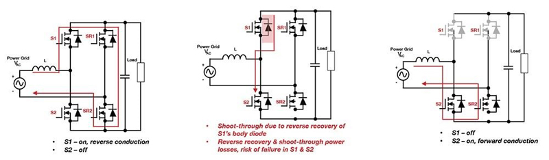
In a typical totem-pole PFC application, the FETs are arranged in a half-bridge configuration as shown in Figure 3. S1 and S2 are high-frequency FETs, while SR1 and SR2 are low-frequency FETs. The high-frequency FETs turn on and off alternately; however, during dead time, the body diode of one of the FETs is conducting (S1). Following this body-diode conduction during dead time when the high-frequency FET (S2) is turned on, the reverse recovery of the S1’s body diode will flow through S2, turning into a shoot-through situation. This is especially unavoidable in continuous-conduction-mode (CCM) PFC applications. However, with no body diode and no reverse-recovery, it would be possible to avoid the risk of shoot-through. That is exactly the benefit that GaN brings to totem-pole PFC because it doesn’t have a body diode.
Click image to enlarge
Figure 3: Pre-conditioning for totem-pole PFC enables very low reverse recovery
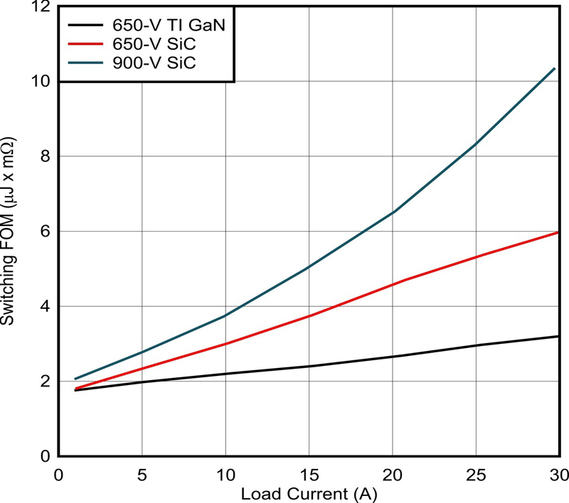
GaN incurs over 50% lower switching energy loss versus comparable SiC MOSFETs. This is primarily due to its higher switching speed capability (100 V/ns or higher), lower parasitic output capacitance and zero reverse recovery. Figure 4 summarizes results from the industry-standard double pulse test used to evaluate the FET energy loss incurred during switching. The test normalized the switching energy loss for each FET to on-resistance and presented the results as a figure of merit.
Click image to enlarge
Figure 4: DPT results comparing TI GaN and 650 V and 900 V SiC MOSFETs
Advantages of TI GaN
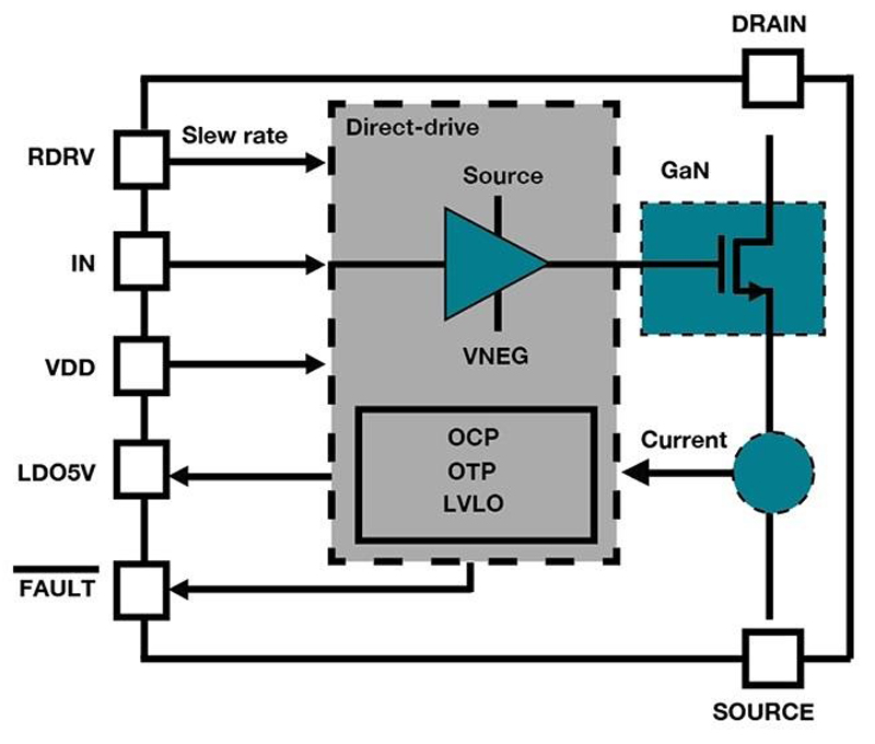
The Texas Instruments (TI) approach to developing GaN technology is different from typical power FETs. TI’s GaN FET, the LMG3422R030, integrates the gate driver, protections and reporting in one quad-flat no lead surface-mount device package. Figure 5 is a block diagram of the LMG3422R030.
Click image to enlarge
Figure 5: Block diagram of the LMG3422R030GaN FET
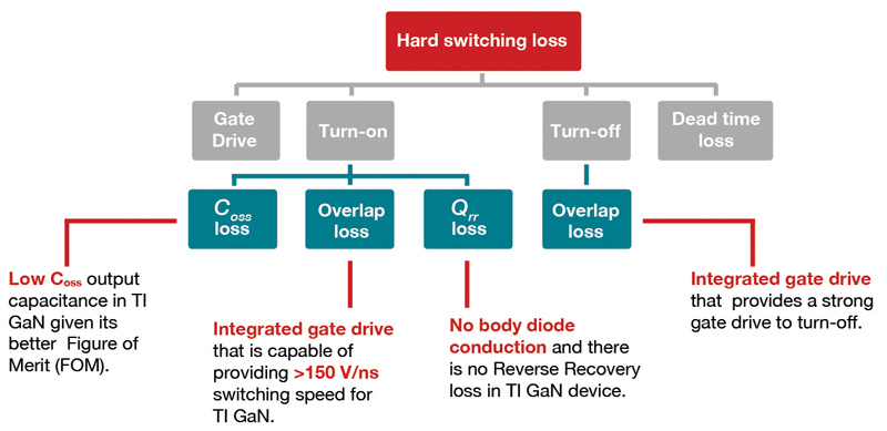
The integration of the driver allows designers to have lower common source and gate loop inductance, enabling switching speeds up to 150 V/ns, which is significantly challenging to achieve in high-frequency designs with discrete components due to concerns such as gate voltage overstress that can degrade FET reliability. Figure 6 shows the benefits of TI GaN in reducing hard-switching losses.
Click image to enlarge
Figure 6: TI GaN reduces hard-switching losses in CCM PFC.
The integrated protection and reporting features help reduce the number of external components needed for a reliable design. These features, along with the inherent benefits of GaN technology, offer advantages that can help reduce the hard-switching losses in CCM PFC during turnon and turnoff, such as output capacitance, overlap and reverse-recovery losses.