Data has been wireless for some time. Now consumers are demanding the ability to charge wirelessly and technology enablers are responding. In this technical article, Infineon will review the current state-of-art and compare the benefits of advanced wireless charging solutions using a totally integrated approach.
Background
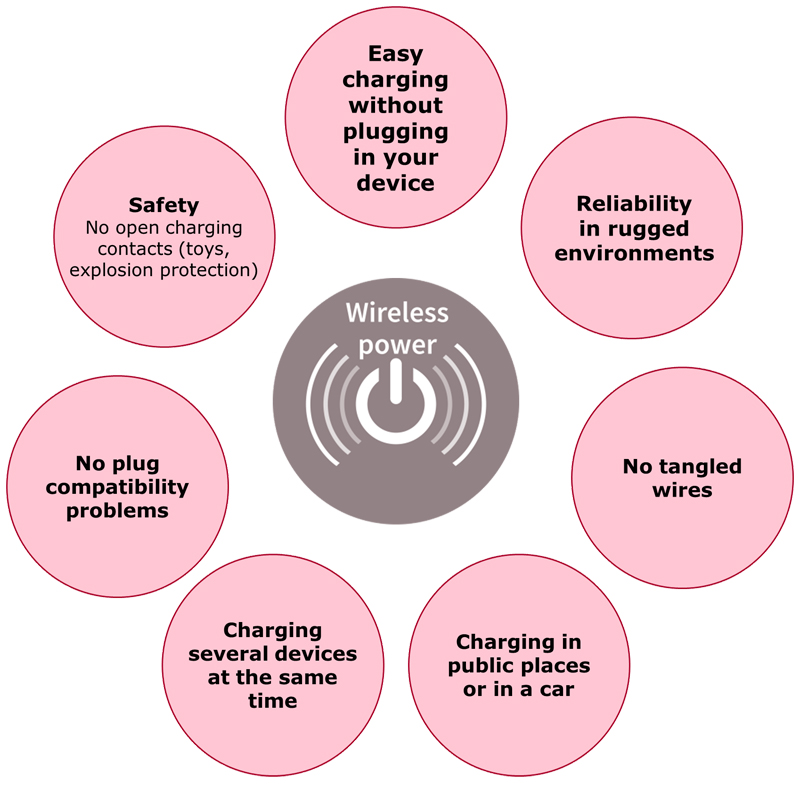
Every electronic device requires power, but few are truly wireless as the power is supplied from a wall outlet via an adapter. The term "wireless" is now synonymous with data transfer. However, wireless electromagnetic fields can also transfer power to a device, delivering even greater convenience for the user. As no cables are required, compatibility issues are reduced and device robustness is increased.
By elimination all connectors, devices are more easily sealed, benefiting rugged applications as well as consumers in general, as around one in five smartphones are accidently dropped into a liquid at some point. The great advantage of wireless charging is to eliminate bulky charger adapters.
As the industry moves to a universal charging solution, iti is likely that more compatible charging stations will appear in airports, hotels, event venues, fast food chains, coffee shops and elsewhere.
Challenges designers face
Most chargers are Switch-Mode Power Supplies (SMPS) that require a good understanding of magnetics - considered by many to be a "black art".
Wireless charging works in a similar way - except the transformer is split between the charger and the device to be charged. As such, the terminology changes - the primary side becomes the "transmitter" and the secondary is now the "receiver".
In wireless charging the coils and their coupling have a greater impact on the overall performance than in an SMPS. As wireless windings are separated the coupling is looser than with a SMPS. However, a good coupler factor and power can be transferred with unexpected efficiency.
Other than magnetics, issues including efficiency, mechanical packaging, electromagnetic interference (EMI), thermal management and metallic foreign objects (such as coins and keys) create further challenges for designers.
Wireless topologies and technologies
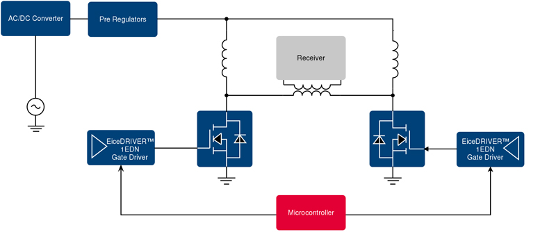
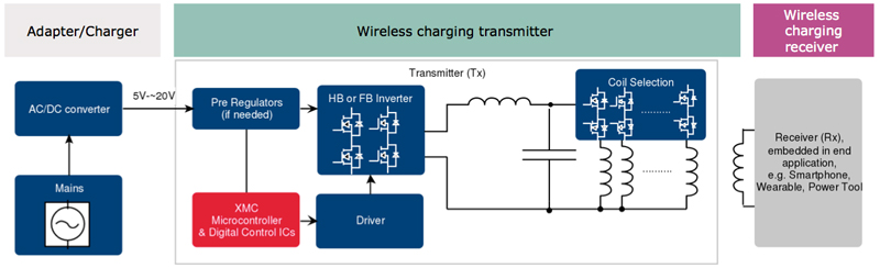
Wireless charging solutions typically have three key elements; the adapter/charger, the transmitter and the receiver as shown below.
Click image to enlarge
Figure 2: Typical wireless charging systems consist of three main elements
The adapter converts the main supply and delivers power to the primary side/transmitter, usually with a 5-20 VDC regulated voltage. Adapters are most often a separate device with a cable connection to the transmitter, although they could equally be combined into a single unit.
The transmitter contains a MOSFET-based half-bridge or full-bridge inverter that converts the DC power into an AC waveform and creates an alternating magnetic field. The inverter is controlled by a microcontroller and associated MOSFET drivers to provide the flexibility and functionality required for inductive wireless charging.
Class D and Class E are two popular topologies for resonant applications. Although quite similar in a number of aspects, each approach offers slightly different benefits making each suitable for different applications.
Click on image to enlarge
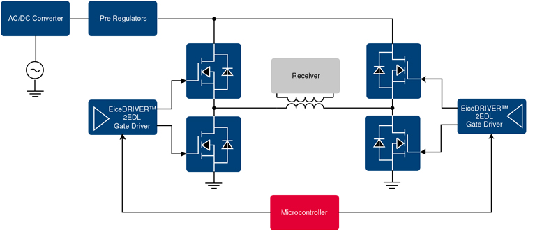
Figure 3: Class D topology for resonant applications
A Class D wireless charging implementation is shown above as a full-bridge topology. A half-bridge topology can also be used. Class D offers an almost-flat efficiency curve over a wide load range and is therefore suited to general-purpose wireless charging stations, such as those found in public places where a wide variety of devices could be charged. This approach is suitable for a wide range of power levels.
Click image to enlarge
Figure 4: Class E topology for resonant applications
A Class E topology is shown above; this can be either a single-ended approach or a differential arrangement (as shown) can be used. Unlike the Class D topology, Class E is optimized for a particular parameter set and, at a certain defined point, will show greater efficiency. However, the Class E efficiency falls off more rapidly away from this point. Therefore, a Class E topology is the best option for higher power levels and for charging of a specific device that is either charged close to target power or not charged at all. Class E BOM costs tend to be slightly lower than those of Class D, but there is not a huge difference.
Infineon Technologies offers a full suite of component solutions for wireless charging transmitters, as well as the associated switched power supplies used to convert the mains AC current into DC which is fed into the inverter.
Key wireless charging-orients products come from throughout the broad range giving design engineers the confidence of using components and subsystems where compatibility is assured.
The microcontroller provides the system control / intelligence and sits at the heart of the transmitter design. Infineon's XMC™ microcontroller product line presents designers with multiple options, although the XMC1100, 1402 and XMC4108 are most suited to the Class D and E topologies that are popular for wireless charging.
The EiceDRIVER™ gate drivers translate the microcontroller signals to directly drive the MOSFETs. The new 2EDL71 is most suited to the Class D designs and the established 1EDN is preferred for Class E applications.
Infineon offer an extensive range of MOSFETs. Choices include options for package size as well as important operating parameters such as RDS(ON) and Qg, where Infineon has the leading Figures of Merit (FoM) in the industry. Multiple voltage classes from 30 V to 250 V are available, giving designers flexibility to use the same base technology to design wireless chargers at multiple power levels. Infineon's market leading OptiMOS™ MOSFETs are used for the Class D or E power inverter (as well as synchronous rectification topologies) and CoolMOS™ devices in CE and P7 versions provide switching capabilities for the ACDC Adapter.
Infineon also offers a range of Flyback controllers for the power adapters that work well alongside the CoolSET™ integrated IC and power stage.
Supporting the component solutions, Infineon's newly developed test board for Class D power amplifier transmitters gets designers started quickly with designing and developing highly efficient and compact solutions.
The test board allows designers to evaluate the functionality and performance of Infineon MOSFETs in a Class D configuration power amplifier. Containing two half bridges constructed with 80 V 2x2 Infineon MOSFETs (IRL80HS120) and the related driver, the test board allows users to switch between single ended configuration (only one half bridge is active) and differential configuration (both half bridges are active).
An embedded oscillator ensures an accurate 6.78 MHz operating frequency, and also provides a pin to set the switching frequency externally with a waveform generator, via a BNC connector.
All of the required components to design the Zero Voltage Switching (ZVS) power solutions are included in order to achieve the highest possible efficiency. An on-board linear regulator provides a stable supply voltage for the board logic.
A second BNC connector allows the connection of an external transmitting coil for wireless power transfer. If a wireless charging capable receiver device is available then a complete wireless charging design can be created.
Summary
Transmitting power wirelessly brings the same benefits enjoyed with data to device charging. As standards and approaches consolidate, users will enjoy increased convenience through greater interoperability between all chargers and portable devices. Continued consolidation and innovation will bring true 'drop and charge' convenience as well as increasing power levels, thereby enabling more device types to be charged wirelessly.
As a leading supplier, Infineon's has a comprehensive product range containing all of the critical components required for the AC adapter and transmitter. Each of the components exhibits high levels of performance, including low switching / conduction losses as well as packages with low levels of parasitics and an excellent FoM for wireless charging that allow designers to realize a solution with mature and reliable silicon MOSFET technology. Infineon's long experience in power semiconductors and microcontrollers has led to them becoming known as a technology and quality leader.
Test boards that speed up evaluation and development back this broad product range that covers all aspects of wireless charging design. Infineon offers an advanced product range as well as a valuable support ecosystem for designers of wireless charging solutions - now and in the future.
TThew
Th
Wirele
Data