Wireless Charging Without the Need for Digital Control
Closing the loop between a wireless charger receiver and transmitter without using digital controllers
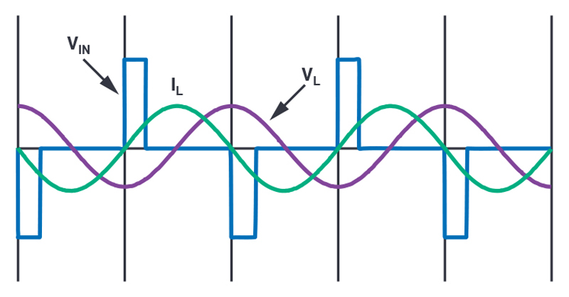
Figure 1. AutoResonant LC tank voltage and current waveforms with square wave input at less than 50% duty cycle
Wireless charging is increasingly utilized for small size wearable devices, as it eliminates the need for cables or any exposed connectors on the device. For applications with charge current less than 10 mA, closed-loop control between the wireless charger receiver and the transmitter is not required as the power dissipationislow.However, for higher charge current, it is essential for the transmitter to actively adjust its output power based on the demands of its receiver and coupling coefficient between the two sides. Otherwise, the receiver may have to dissipate the extra power in the form of heat, impacting the user experience and posing a threat to the health of the battery. Digital communication from the receiver to the transmitter is usually used to close this loop, but digital control adds complexity in overall design and increases the size of the application.
This article introduces a method for closing the loop between the receiver and the transmitter without increasing the number of components (and precious overall footprint) on the receiver board. A closed-loop, controlled wireless charger prototype is built using an LTC4125 Auto Resonant transmitter and an LTC4124 wireless Li-Ion charger receiver to demonstrate this concept.
AutoResonant transmitter with a duty cycle control input
The LTC4125 is a monolithic, full-bridge Auto Resonant wireless power transmitter designed to maximize the available power to the receiver, increase the overall efficiency, and provide thorough protection to the wireless charging system.
The LTC4125 implements an AutoResonant converter to drive the series-resonant tank composed of the transmit coil (LTX) and the transmit capacitor (CTX). The Auto Resonant driver uses a zero-crossing detector to match its driving frequency with the resonant frequency of the tank. The SW1 and SW2 pins are the outputs of the two half-bridges inside the LTC4125. When the SWx pin senses the direction of its output current crosses zero from negative to positive, SWx is set to VIN for a duty cycle that is proportional to its corresponding PTHx pin voltage. When the SWx pin is set to VIN, current flowing in the transmitter resonant tank is increased. Therefore, the duty cycle of each bridge driver controls the amplitude of the tank current, which is in proportion to the transmit power. Figure 1 shows the tank current and voltage waveforms with a duty cycle less than 50%. The absolute value of the tank current amplitude is determined by the overall tank impedance, including the reflected load impedance from the wireless receiver.
In typical operation, the LTC4125 sweeps the SWx duty cycle using an internal 5-bit DAC that sets the PTHx voltage to search for a valid load. If the FB pin sees certain patterns of voltage change, the sweep is stopped, and the duty cycle stays at that level for a programmable time period (usually set to around 3sto5s). Then a new sweep cycle starts, repeating the same steps. If the load condition is changed during a sweep period, the LTC4125 will respond at the beginning of the next sweep period.
To form a closed loop, the transmit power of the bridge driver should adjust based on control input. One of the features in the LTC4125 is that the PTHx pin is not only an indicator of the bridge driver duty cycle, but can also be driven as an input to set the duty cycle. The internal 5-bit DAC sets the voltage target of PTHx pin with an internal pull-up resistor. An external pull-down resistor in series with a FET can be implemented to actively discharge a capacitor on PTHx pin, thus reducing the PTHx pin average voltage. The duty cycle of the PWM signal at the gate of this pulldown FET controls the average voltage on PTHxpin.
The LTC4125 is designed to deliver over 5 W to a proper receiver. When paired with the LTC4124 receiver, the transmit power can be reduced by deactivating one of the half-bridge drivers. This is done by leaving the SW2 pin open and PTH2 shorted to GND. The transmit resonant tank can then be connected between SW1 pin and GND. In this way, the LTC4125 becomes a half-bridge transmitter to allow for a lower gain and wider control range on the PTH1 pin.
Generate Feedback Signal from the Wireless Charger Receiver Using LTC4124
The LTC4124 is a highly integrated 100 mA wireless Li-Ion charger designed for space-constrained applications. It includes an efficient wireless power manager, a pin programmable, full-featured linear battery charger, and an ideal diode Power Path controller.
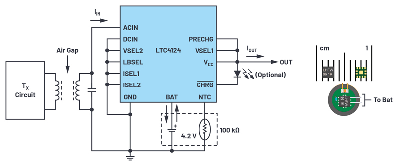
Click image to enlarge
Figure 2. A complete wireless battery charger solution using the LTC4124 on a 6 mm application board
The wireless power manager in the LTC4124 connects to a parallel resonant tank via an ACIN pin, allowing the linear charger to receive power wirelessly from an alternating magnetic field generated by a transmit coil. When the LTC4124 receives more energy than it needs to charge the battery at the programmed rate, the input capacitor of the linear charger on the VCC pin is charged up to absorb the extra energy. When the VCC pin voltage reaches 1.05 V over the battery voltage, VBAT, the wireless power manager shunts the receiver resonant tank to ground, until the VCC falls back down to 0.85V over VBAT. In this way, the linear charger is highly efficient as its input is always kept just above its output.
The shunting event of the LTC4124 also reduces reflected load impedance on the transmit resonant tank, causing the amplitude of transmit tank current and voltage to rise. As the shunting event indicates the receiver is getting enough power from the transmitter, the rise of the transmit tank peak voltage can serve as a feedback signal for the transmitter to regulate its output power.
Demodulate the Feedback Signal and Close the Loop
Now that feedback signal from the receiver side is available on the transmitter side, this feedback signal needs to be translated and fed into the control input of the transmitter to close the control loop. The peak tank voltage can be obtained from a half-wave rectifier consisting of a diode and a capacitor CFB1, as shown in Figure 3. This voltage is further divided by resistors RFB1 and RFB2. To sense the change of the peak current, the peak voltage signal is averaged via a low-pass filter formed by a resistor(RAVG) and a capacitor (CAVG). By comparing this average signal to the original peak voltage signal, a square wave pulse can be generated. This pulse is then fed into the duty cycle control input of the LTC4125 to regulate the output power of the transmitter.
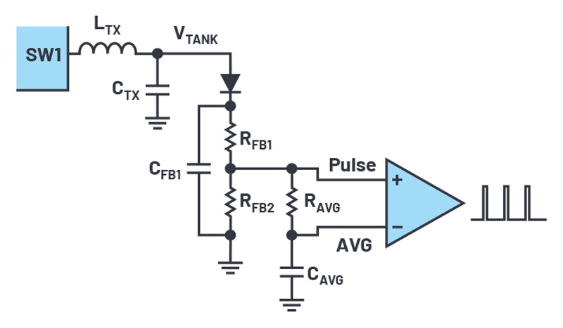
Click image to enlarge
Figure 3. Feedback signal demodulation circuit on the transmitter side
When the receiver is not getting enough energy, the LTC4125 should increase its output power. This can be achieved by setting the internal voltage target for the PTHx pin. The internal voltage target can be set by the PTHM pin as it sets the initial 5-bit DAC voltage level before the start of the LTC4125 search period. A 1 V voltage reference can be connected on IMON pin to disable the search, keeping the PTHx pin target voltage fixed at its initial value during the operation. If the LTC4124 receiver demands more power, the shunting event will stop and the PTHx discharging FET will not be activated. The PTHx voltage will be charged toward the internal voltage target until the LTC4124 receives enough power to start the shunting event.
The maximum transmit power is defined by measuring the PTHx voltage when the receiver is regulating maximum charge current at the worst coupling coefficient position in the application. The PTHM pin voltage should be set to meet the maximum transmit power requirement.
Features and Performance of the Closed-Loop Wireless Charger
Figure 4 shows the complete schematic for the LTC4125-based closed-loop controlled transmitter and the 100 mA LTC4124-based receiver. As shown in the schematic, very few components are required on the receiver side, lowering the cost and reducing the volume of the receiver. On the transmitter side, compared to the LTC4125 typical applications, only a few additional components are used to achieve the closed-loop control. Most of the features for the LTC4125 are retained, including AutoResonant switching, multiple foreign detection methods, overtemperature protection, and resonant tank overvoltage protection. Details of these features can be found in the LTC4125 datasheet.
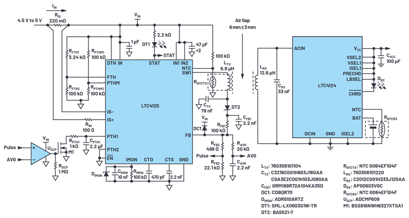
Click image to enlarge
Figure 4. 100 mA LTC4124 charger receiver paired with LTC4125 AutoResonant closed-loop controlled transmitter
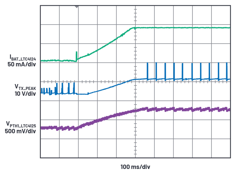
The LTC4125-based closed-loop wireless transmitter can dynamically adjust its output power to match the power demand by the receiver. Figure 5 shows the behavior of this wireless charger when the receiver coil is moved away from the center of the transmitter coil and then quickly moved back to the original position. The output power of the LTC4125 transmitter, which is indicated by the peak transmit tank voltage VTX_PEAK, responds smoothly to the change of the coupling coefficient between the two coils to keep the charge current constant.
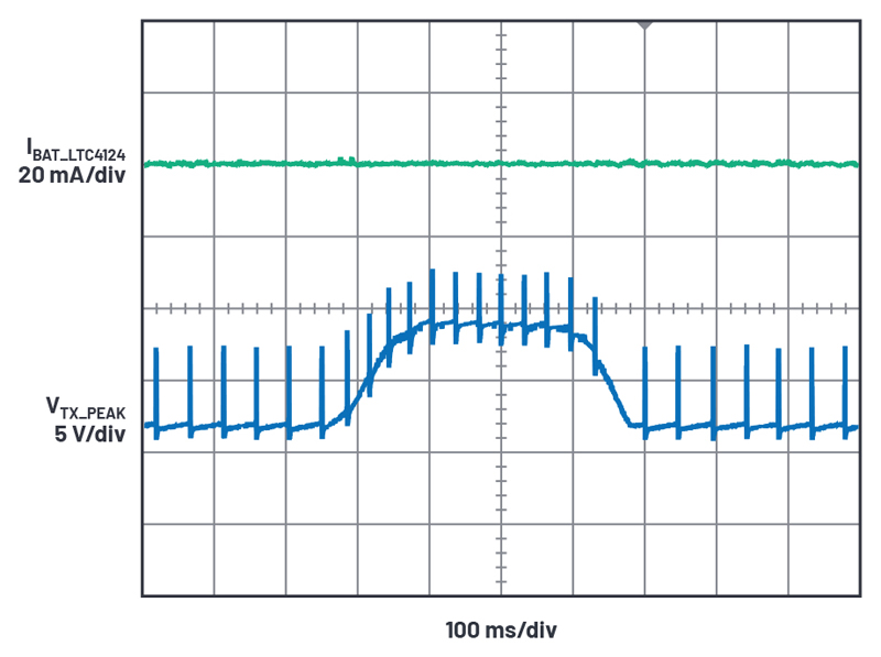
Click image to enlarge
Figure 5. The LTC4124-and LTC4125-based closed-loop wireless charger response to a sudden change of the coupling coefficient between the transmitter and receiver
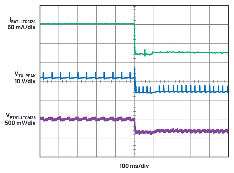
During a charge current rise transient, the LTC4124 shunting event stops, allowing the LTC4125 to charge up its PTH1 pin internally. As a result, the LTC4125 increases its half-bridge driver duty cycle to boost the transmit power. Once the transmit power is large enough for the LTC4124 to regulate its charge current, the shunting event resumes and the duty cycle remains at an optimum level. During a charge current fall transient, the LTC4124 shunts much more frequently. The LTC4125 quickly discharges the capacitor on its PTH1 pin to lower the duty cycle and reduce the LTC4125 transmit power.
Click image to enlarge
Figure 6. The LTC4124- and LTC4125-based closed-loop wireless charger response to a step up in charge current
Click image to enlarge
Figure 7. The LTC4124- and LTC4125-based closed-loop wireless charger response to a step down in charge current

Click image to enlarge
Figure 8. Zoomed-in waveform to show detail of the transient shown in Figure 7
Click image to enlarge
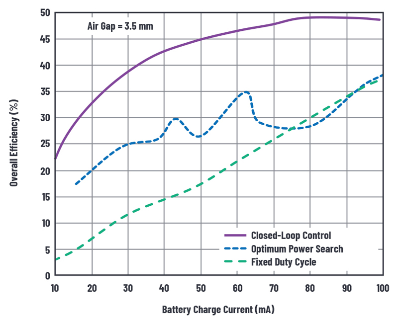
Figure 9. Efficiency of various configurations of the LTC4125- and LTC4124-based wireless charger at 3.5 mm air gap
As the transmit power always matches the demand of the receiver, the overall efficiency is greatly improved compared to typical configurations of a LTC4124- and LTC4125-based wireless charger without closed-loop control. The efficiency curve is smoother without the internal DAC steps in the LTC4125 optimum power search operation. As power loss is greatly reduced, the LTC4124 charger and the battery remains near room temperature throughout the charging period.