Zero-crossover-distortion amplifiers improve linearity of DAC Systems
Used in many applications, digital-to-analog converters are often accompanied by an amplifier
Digital-to-analog converters are widely used in many different applications and an amplifier often accompanies them to signal-condition the output. The amplifier functions to increase output current drive, to convert differential to single ended output, to isolate the downstream signal path, or to provide a complementary bipolar output voltage. Figure 1 shows a typical section of a single supply signal chain, consisting of a voltage reference, a digital-to-analog converter, and a buffer. To maintain a high dynamic output range and high signal-to-noise ratio, digital-to-analog converters (DACs) are often designed to operate full swing, where the reference voltage (VREF) is set equal to the supply voltage (VDD). This allows maximum usage of the digital codes. With a single supply, the DAC and the output buffer power supply are often connected to the same supply line. In this configuration, a rail-to-rail input and output amplifier is required to buffer the converter.
Click image to enlarge
Figure 1. Typical section of a single supply signal chain
A classic non rail-to-rail input amplifier uses a p-type (or n-type) differential pair at its input stage. The p-type input amplifiers allow input common-mode voltage to reach and include the lower supply rail. This is especially useful in ground sensing application. On the other hand, the n-type input amplifiers allow input voltage to range from a few Volts above the lower supply rail to the upper supply rail. Such amplifiers suit applications that need to include the upper supply rail, for example, high side current sensing monitors. To enable the input common-mode voltage to extend to both supply rails, rail-to-rail input amplifiers incorporate both n-type and p-type input stages.
The majority of rail-to-rail input amplifiers are designed using two input differential pairs in parallel, an n-type and a complementary p-type. The input common-mode voltage determines which differential pair turns on and is active. The p-type differential pair turns on when the input voltage approaches and reaches the lower supply rail. The n-type pair is active for input voltages up to and including the upper supply rail. This topology allows the amplifier to maintain a wide dynamic input voltage range and maximize signal swing to both supply rails. However, these amplifiers exhibit a trade-off – a unique characteristic generally known as ‘crossover distortion’.
Input differential pairs commonly exhibit different offset voltages. The handoff from one pair to the other due to input common-mode voltage change creates a step-like characteristic that is visible in the graph of offset voltage vs. input common-mode voltage. This crossover distortion is inherent to all rail-to-rail input amplifiers designed with the dual differential pair topology. Refer to Figure 2 for an example. For this amplifier running on +5V and ground, the crossover region occurs at 3.4 Volts of input common-mode voltage. Such an amplifier is used in applications where the input voltage range goes rail to rail, but can pose a problem when the input common-mode voltage is at the transition region. As an example, this unique characteristic causes nonlinearity when the amplifier is used as a buffer for a DAC output.
Click image to enlarge
Figure 2. Input offset voltage vs. input common-mode voltage of a typical rail-to-rail input amplifier
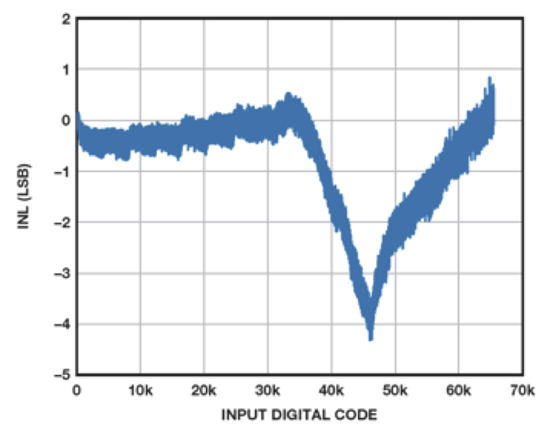
Figure 3 shows the integral nonlinearity (INL) error of a circuit using a 16 bit digital-to-analog converter and a typical rail-to-rail input and output buffer. INL error is the deviation (in LSBs) of the actual converter transfer function from an idealized transfer function. Note that the input of the digital-to-analog converter is swept from code 200 to code 216-200. Approximately 15mV (200 codes) from either end of the range is excluded because a rail-to-rail output amplifier is not truly rail to rail out and require some output headroom (usually specified in the data sheet). The crossover distortion is detected at an input digital code of about 45000. This corresponds to an input common-mode voltage of 3.4V. Clearly, the amplifier crossover distortion degrades INL, affecting system accuracy. In this particular example, the crossover nonlinearity is as high as 4 to 5 LSBs for a 16-bit system. Many systems perform calibration to remove initial offset voltage, but such nonlinearity cannot be removed by calibration.
Click image to enlarge
Figure 3. Integral nonlinearity (INL) of a 16 bit DAC and a typical rail-to-rail input buffer companion
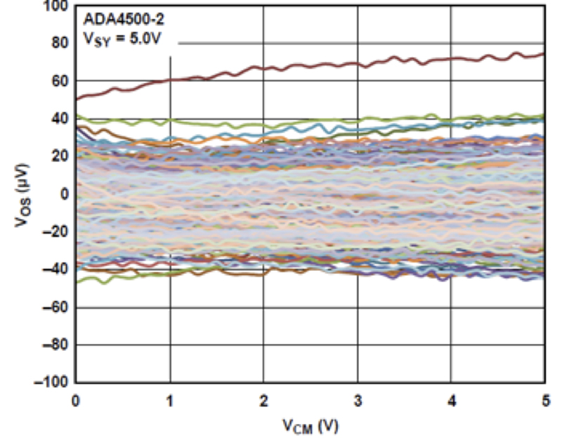
Crossover nonlinearity can be resolved by using a zero-crossover-distortion amplifier. This type of amplifier integrates a charge pump input enhancement circuit on chip to achieve rail-to-rail input swing. The charge pump increases the internal supply by a few Volts to provide the headroom needed for the input stage; the amplifier then achieves rail-to-rail input swing without the need for a complementary input differential pair. Consequently, it does not exhibit crossover distortion. An example of a zero-crossover-distortion amplifier is Analog Devices’ ADA4500-2. Figure 4 shows the offset voltage vs. input common-mode voltage of the device. Notice that offset voltage is quite constant over the input common-mode voltage range.
Click image to enlarge
Figure 4. Offset voltage vs. input common-mode voltage of a zero-crossover-distortion amplifier
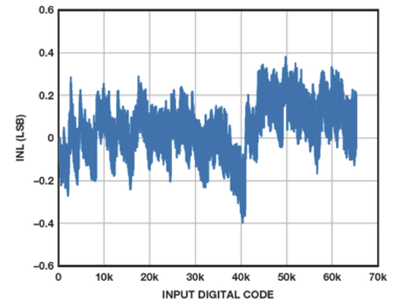
Using a zero-crossover-distortion amplifier eliminates crossover nonlinearity in a digital-to-analog converter system. Figure 5 shows the INL of a circuit using the same 16 bit digital-to-analog converter and the ADA4500-2. The zero-crossover-distortion feature improves INL to less than +/-1LSB.
Click image to enlarge
Figure 5. Integral nonlinearity (INL) of a 16-bit DAC and the ADA4500-2
As an alternative to using a zero-crossover-distortion amplifier to avoid crossover nonlinearity, one could also supply the converter with a reference voltage (VREF) that is lower than its supply (VDD). For example, use a 2.5V reference voltage with a 5V supply. This would ensure that the crossover region of a typical rail-to-rail input amplifier is out of the input digital code range. As a tradeoff, this halves the output range. An external amplifier might also be needed to amplify the output if the signal level is too low. Another option, if the system has multiple supplies, is to provide the amplifier with a higher power supply, allowing the use of a non-rail-to-rail input amplifier. The increase in power supply would provide enough headroom for the input stage. This however would be less power efficient.
All in all, it is important to carefully consider the appropriate amplifier as a DAC output buffer. You can use a lower DAC reference voltage at the expense of a reduced output range, or increase the buffer supplies at the expense of higher power consumption. Better yet, you can use a rail-to-rail input and output amplifier to maximize input and output range, but consider using a zero-crossover-distortion amplifier to avoid errors that come from crossover nonlinearity.