IBM develops 2 nm process
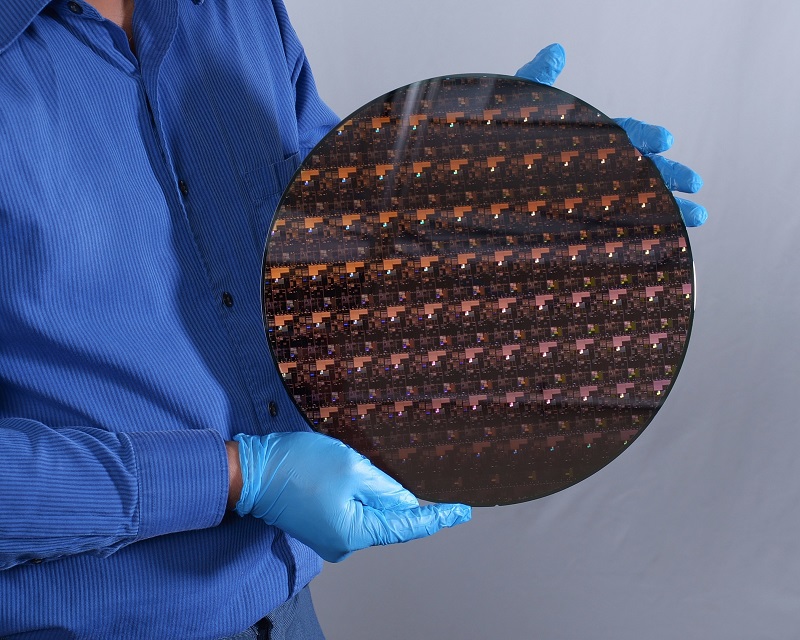
IBM has announced this week that it has developed a 2 nm process technology - the smallest chip geometry in the industry by quite some way. It’s not the first time that Big Blue has made the news in IC manufacturing recently, as the company was also at the forefront of the development of 7 nm and 5 nm technology nodes. Although we expect innovation from IBM, the reason the development is quite unusual is that the company sold all their fabs 7 years ago to GLOBALFOUNDRIES and only work with partners on process technology these days. These partners include Intel and Samsung, as well as GLOBALFOUNDRIES.
IBM claims that the new process node will offer up to 45% more performance and use up to 75% less power than the most advanced 7 nm node available at the moment. The process is based on nanosheet technology, which was developed by IBM in collaboration with GLOBALFOUNDRIES and Samsung. The process uses stacks of silicon nanosheets as the device structure of the transistor instead of the standard FinFET architecture. Extreme Ultraviolet (EUV) lithography allows the width of the nanosheets to be adjusted within a single manufacturing process. This provides the ability to fine-tune the performance and power for specific circuits, as opposed to FinFET transistor architecture, which is limited by the current-carrying fin height. Although IBM claims the process node is 2 nm, no features of the transistor is actually that size. When the industry moved from 2D to 3D technologies, like FinFET, the relevance of measuring process nodes by gate size was lost, and now the technology nodes are based on the estimated size of an equivalent 2D architecture.
The technology will mainly be used, at least initially, for advanced processors, memory chips and SoCs, so the announcement will not affect the power industry directly for a long time. However, IBM’s claim that it could use up to 75% less power should ensure that the power density does not create too much of a problem for those tasked to design the circuits that will power it. According to Anandtech, the density of transistors is about double that of TSMC’s 5 nm technology. It may be some time before we see the technology in commercial applications as the IBM Research 7 nm nanosheet process advancements have still to appear on the market at all so far. The first chips to use the technology are scheduled for use in IBM POWER10-based systems that will be launched later this year.
The race against Moore’s Law has always fascinated me. Every time you think that it is coming to an end, there is an advancement that pushes the boundaries even further. At some points in the race for smaller geometries, the advancements have seemed more like magic than physics or chemistry. Fewer and fewer companies can compete now due to the cost of fabricating the new nodes, but with the US and EU seemingly determined to bring chip manufacture back from foreign shores, who knows where the next innovation may spring up from?
.jpg)
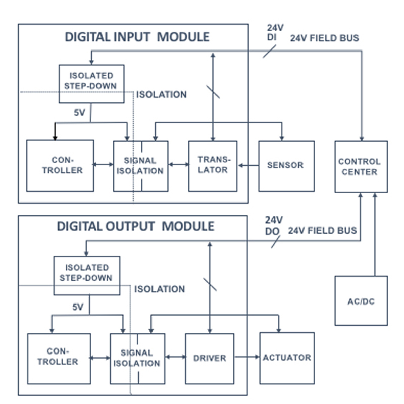
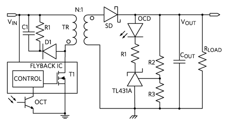
Accelerating Isolated Power Supply Design
05/10/2017