Industrial
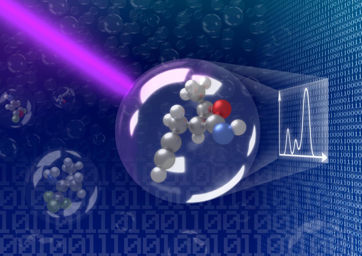
ARTIST, which stands for Artificial Intelligence for Spectroscopy, instantly determines how a molecule will react to light.
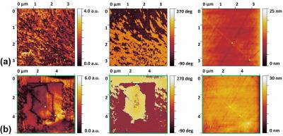
Ferroelectric single-crystal-architecture-in-glass is a new class of metamaterials that would enable active integrated optics if the ferroelectric behavior is preserved within the confines of glass. We demonstrate using lithium niobate crystals fabricated in lithium niobosilicate glass by femtosecond laser irradiation that not only such behavior is preserved, the ferroelectric domains can be engineered with a DC bias. A piezoresponse force microscope is used to characterize the piezoelectric and ferroelectric behavior. The piezoresponse correlates with the orientation of the crystal lattice as expected for unconfined crystal, and a complex micro- and nano-scale ferroelectric domain structure of the as-grown crystals is revealed.
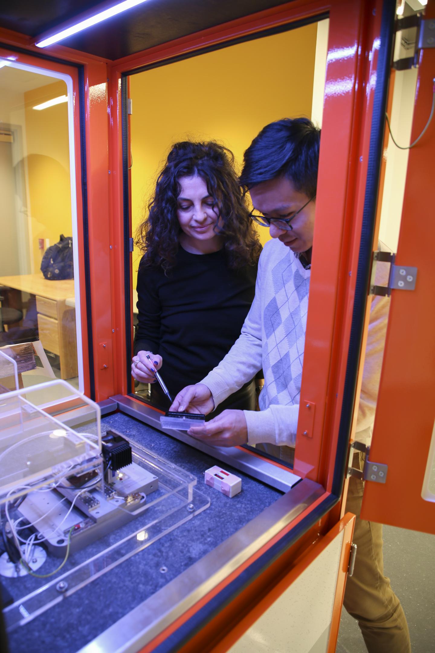
In the NYU Tandon School of Engineering PicoForce Lab, Professor Elisa Riedo and doctoral student Xiangyu Liu fabricate high-quality 2D chips using the thermal scanning probe lithography process they invented and NanoFrazor equipment by SwissLitho. The process holds promise as an alternative to today's electron beam lithography.

Graphene Flagship researchers reviewed the current research into the safety of graphene and related materials

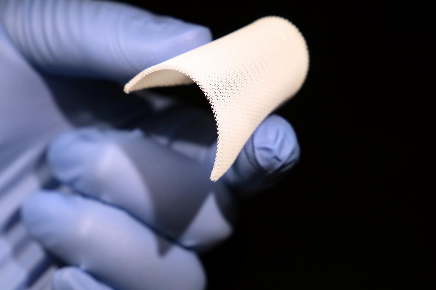
A printed flexible sheet of piezoelectric smart material


Click image to enlarge
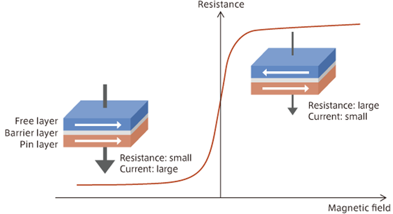
Figure 1. Principle of TMR
As the magnetization directions of the pin layer and free layer are parallel, the resistance becomes small and current flows with little resistance. When the magnetization directions of the pin layer and free layer are not parallel, resistance increases which limits current flows.

Click image to enlarge
Figure 1: Predictive Maintenance Market Share 2017-2022
Click image to enlarge
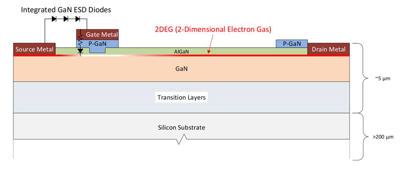
Figure 1 Cross section of a 600 V CoolGaN™ ™ power transistor [1]


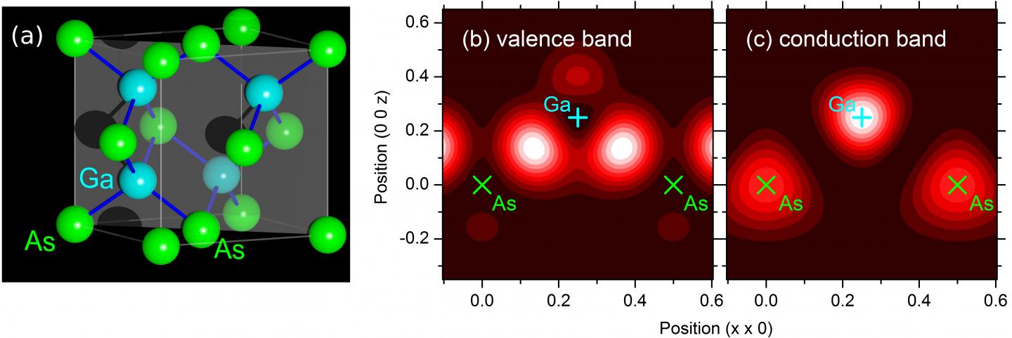
(a) Unit cell of the semiconductor gallium arsenide (GaAs). Chemical bonds (blue) connect every Ga atom to four neighboring As atoms and vice versa. Valence electron density in the grey plane of (a) in the (b) ground state (the electrons are in the valence band) and in the (c) excited state (electrons are in the conduction band). Apart from the valence electrons shown, there are tightly bound electrons near the nuclei.
How can a computer learn to generalize the knowledge contained in a huge dataset and find solutions for complex problems on its own? This question is the focus of two new assistant professorships.

Your knees and your smartphone battery have some surprisingly similar needs, a University of Michigan professor has discovered, and that new insight has led to a 'structural battery' prototype that incorporates a cartilage-like material to make the batteries highly durable and easy to shape.