DARPA, has partnered with a Princeton-led initiative to reimagine how AI processing is accomplished
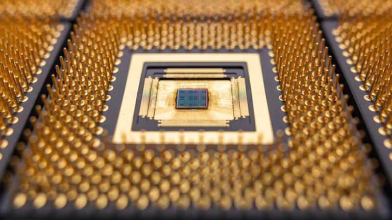
There’s no doubt that AI will be the next big thing in technology, if it isn’t already. Most large AI installations are powered by basically the same GPUs (graphical processing units) that are found in gaming PCs. That demand has seen leading GPU supplier Nvidia’s value explode to become only the third company in the world to reach a valuation of $2 trillion. However, AI implementation is using larger models than ever, and these continue to grow as AI is deployed onto more complex tasks. This means that both powering racks of the advanced chips and getting data to and from memory are becoming bottlenecks in the process. AI processing is also usually accomplished in data centres, where that processing power can be concentrated, and not where it is required and is most useful.
As the name suggests, GPUs have been designed primarily to manipulate graphics. They are ideal for that task, but also the best architecture that we currently have for processing AI. However, a dedicated AI device could theoretically process AI workloads more efficiently in terms of both processing and power usage. But, solutions based on today’s technology would soon run into the same problems that GPUs face getting data to and from the chip and powering it. Therefore, a completely new type of chip may be required if we are to get the best out of AI, and definitely if we want to operate complex AI installations outside of the data centre.
To try and develop hardware that can run AI systems using much less energy, the US Defense Department’s largest research organization, DARPA, has partnered with a Princeton-led initiative, led by Naveen Verma, a professor of electrical and computer engineering. The researchers had to reimagine the physics of computing while designing hardware that can be manufactured with existing fabrication techniques and work well with existing computing technologies.
The project will mainly target inference – chips that process the AI workload once they have already been trained. Verma and his team turned to an alternate approach to the problem: analog computation. His team has discovered a way to accomplish highly accurate computation using the analog signal generated by capacitors specially designed to switch on and off with extreme precision. Unlike semiconductor devices such as transistors, the electrical energy moving through capacitors doesn’t depend on variable conditions like temperature and electron mobility in a material.
“They only depend on geometry,” Verma said. “They depend on the space between one metal wire and the other metal wire.” And geometry is one thing that today’s most advanced semiconductor manufacturing techniques can control extremely well.
DARPA will support Verma’s work with an $18.6 million grant. The DARPA will be used to investigate how fast, compact and power-efficient the new chip can get. The announcement came as part of a broader effort by DARPA to fund “revolutionary advances in science, devices and systems” for the next generation of AI computing. The program, called OPTIMA, includes projects across multiple universities and companies. Its call for proposals estimated total funding at $78 million, although DARPA has not disclosed the full list of institutions or the total amount of funding the program has awarded to date.
In the Princeton-led project, researchers will collaborate with Verma’s startup, EnCharge AI.
.jpg)