Cambridge GaN Devices has developed a technique that allows GaN transistors to be driven in exactly the same way as silicon transistors
The benefits of GaN technology are clear to see. Higher frequency switching means higher efficiency, as well as allowing supporting components to be smaller, giving a more compact design overall. The inherent heat handling properties of GaN devices, coupled with their higher efficiency leads to less heat dissipated, and that also helps with smaller designs by not requiring as much thermal management. GaN devices are more rugged, leading to longer useable lifetimes. There is only one real downside to GaN and that is it does not have the same ease of use as silicon transistors.
There have been many attempts to overcome this hurdle and several different approaches have had some success, allowing the technology to be used, even if it is not at optimal performance. These approaches usually involve adding additional components or customised gate drivers to ensure that the GaN transistors operate safely and reliably. The most popular approach is to embed a full gate driver into the GaN transistor’s package. However the main drawback to this approach is that as the power increases, the losses increase as well.
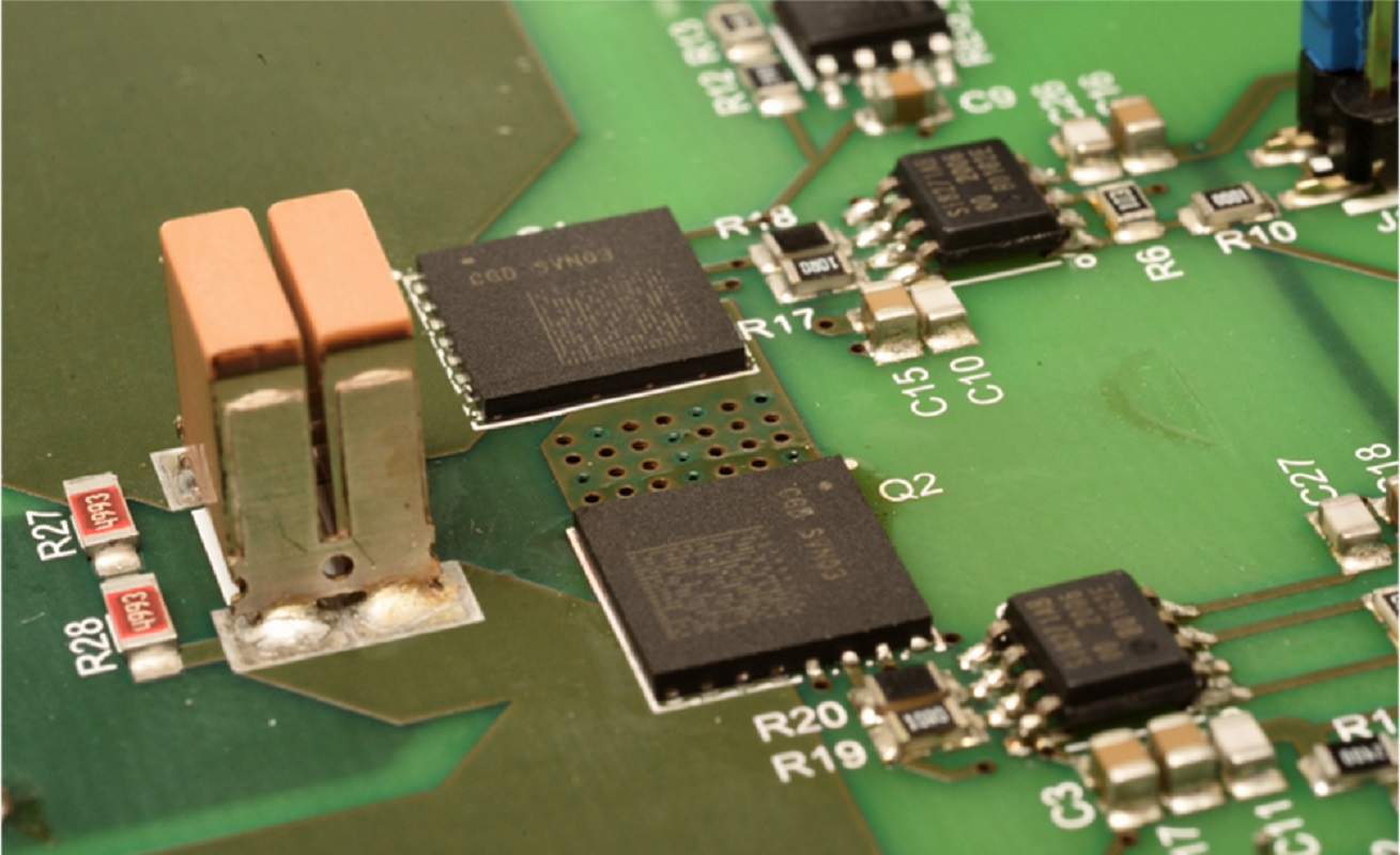
The latest attempt to make GaN easier to use comes from Cambridge GaN Devices (CGD), a company that has been spun-out from Cambridge University. The company claims its new IceGaN (Integrated Circuit Enhancement Mode GaN) technology is the first enhancement-mode GaN transistor that can be operated like a silicon MOSFET without the need for special gate drivers, driving circuitry, or unique gate-voltage-clamping mechanisms. CGD’s GaN devices can be operated with standard gate drivers, up to 20 to 22 V. With a built-in Miller clamp and a threshold voltage set at around 3 V, users don’t need to provide negative gate voltages to keep the device OFF when it's supposed to be OFF.
Rather than add extra components to the circuit, CGD’s technique involves packaging multiple components into the package itself that take the input signal and accurately translate it to the signal required by the gate of the GaN transistor. Andrea Bricconi CGD’s VP of Business Development further explains, “We call our devices a system on chip as it is not just the power transistor, there are several ICs integrated that basically translate the gate signal that comes from the outside to what is needed to drive the embedded GaN gate. We suggest to customers that the drive the GaN transistor exactly like a MOSFET, with no additional components.”
The patented ICeGaN technology is an integrated solution that combines the ease-of-use of Cascode configurations with the simplicity of a single die eMode (normOFF) HEMT and can cut power losses by half over a legacy silicon die. The package also offers a number of integrated smart sense and protection features. The ICeGaN technology can be used in any application that operates in the 650 V market segment. CGD has currently launched four 650 V devices that have RDS(on) from 55 to 200 mΩ and current handling capabilities from 8.5 to 27 A.
https://camgandevices.com/
.jpg)