
Analog Devices’ 3rd generation of Silent Switcher devices have been developed to compete with linear regulators at low frequencies
Switching regulators are the most efficient way of performing power conversion, but they have one large drawback, and that is that they tend to introduce conducted and radiated electromagnetic interference (EMI) into the circuit. This problem becomes acute as systems with sensitive signal paths are used more widely in a range of applications. Of course, manufacturers have not been slow to try to reduce the noise problem. Analog Devices has been developing its Silent Switcher devices for around a decade, and has just made available its 3rd generation of the technology.
Initially, the company tackled the noise issue by splitting the design into two symmetrical signal paths. This meant that when the current flowed in one half of the critical path of the design, it would generate a magnetic field in one direction, and the other half of the circuit would generate an opposing magnetic field. The two magnetic fields effectively cancelled each other out.
The second big innovation that the company made in the initial Silent Switcher family was the incorporation of flip-chip technology. This technique connects the die to the outside world using pillars instead of bonding wires, which removes the majority of the parasitic inductance created. Analog Devices but believes it was the first to use flip-chip technology to generate lower noise in switching power supplies.
The Silent Switcher technology brought other benefits, as Frederik Dostal, Subject Matter Expert, Power Management at Analog Devices explains, “Taking the vast majority of the electrical noise out of the circuit meant that it was then possible to switch the MOSFETs much faster, and that meant lower switching losses and higher conversion efficiency. Some parts can switch at up to 10 MHz making the inductor tiny, and still the EMI is not particularly high”.
Compared to the first generation, the second generation of the Silent Switcher technology was an evolution rather than a revolution. However, it still brought some valuable improvements that made the device simpler to integrate into a design, cut the bill-of-materials and reduce noise further. To accomplish this, the company integrated more of the circuit inside the device, including the four bypass capacitors. This reduced the generated noise further by placing the bypass capacitors closer to the die rather than outside the package to reduce lead frame inductance and the trace inductance of the package.
The new design also had the advantage that it gives designers much more flexibility. Dostal expanded by saying, “Previously when designing the switch-mode power supply board layout, the input capacitor had to be placed as close as possible to the buck regulator input pin and the ground pin, but now it doesn't matter how far away it is. Because the high frequency bypassing is being done internally, and there is very little noise being generated, the bulk input capacitor can be placed further away. It's now very difficult to mess up the board layout”.
The third and latest generation of Silent Switcher products tackles a different problem. The first and second generation devices are ideal for applications that need high-frequency noise eliminated, however at switching frequencies between 0.1 Hz and 100 kHz some noise still remains. Low noise at low frequencies is important for certain applications, such as RF power supplies, instrumentation and medical imaging. These types of applications currently almost always use an ultra-low-noise linear regulator. To target such noise sensitive loads, ADI designed the third generation Silent Switcher devices using voltage reference circuitry that was patented by Linear Technologies in the past and that had previously been used in the company’s ultra low noise linear regulators. The result was a device that offered the benefits of a switching regulator with the low-frequency noise output of a linear regulator.
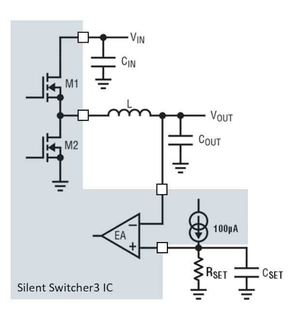
Figure 1 - The new voltage reference circuit in the Silent Switcher 3 series
Dostal explains, “The output voltage is connected directly to the error amplifier. An internal current source drives a current through a resistor, setting the voltage. A small capacitor is placed in parallel with the resistor to help reduce the noise. Noise is therefore reduced on the reference voltage which regulates the output voltage. In other architectures, if the output voltage is set higher, the noise will also increase proportionately. This new architecture doesn’t scale the noise up with output voltage, so it is possible to get extremely low noise throughout the frequency range, even at different voltages that can be set independently of the actual output voltage”.
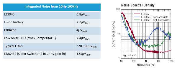
Figure 2 - A comparison of the integrated noise of different devices at lower frequencies
There are currently six members of the Silent Switcher family available. As well as low noise, the devices also feature ultra-fast transient response, as well as many other features.
.jpg)