New Carrier Doping Technique Enhances PV Device Performance
Researchers, led by Tokyo Institute of Technology, demonstrate new method of increasing hole concentration in Perovskite materials
Perovskite solar cells are looked upon as the potential basis of the next generation of photovoltaic (PV) devices. Experimentally, they have shown that have the potential to be a cost-effective and easily manufacturable way of boosting the efficiency of solar cells. However, there are still challenges that remain to be overcome before we see them in widespread use. One of those challenges concerns the hole transport layer (p-type semiconductor) in photovoltaic cells that carries holes generated by light to the electrode. In conventional p-type organic transport semiconductors, hole dopants are chemically reactive and degrade the photovoltaic device. Inorganic p-type semiconductors, which are chemically stable, are promising alternatives, but their fabrication requires high temperature treatment. P-type inorganic semiconductors that can be fabricated at low temperatures and have excellent hole transport ability are more desirable, if they can be produced.
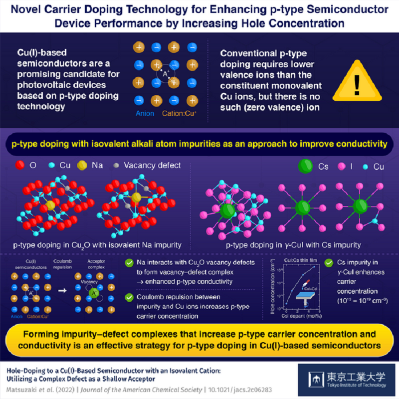
One of the leading candidates for this type of hole transport material is inorganic p-type copper iodide (CuI), which has native defects that give rise to charge imbalance and free charge carriers. However, the overall number of defects is generally too low for satisfactory device performance. Adding impurities with positively charged or donor negatively charged properties, known as “impurity doping,” is the normal method for bolstering the transport properties of semiconductors. In conventional methods, ions with lower valency than the constituent atoms have been used as such impurities. However, in Cu(I)-based semiconductors, there is no ion with a valence lower than that of monovalent copper ions (zero valence), and thus a p-type doping in copper compounds has not been established. Attempting to fill this role, researchers from Japan and USA recently focused on the alkali impurity effect, which has been empirically used for hole doping in copper monovalent semiconductors, copper oxide (Cu2O) and Cu(In,Ga)Se2.
In a study published in the Journal of the American Chemical Society, the team, led by Dr. Kosuke Matsuzaki from Tokyo Institute of Technology (Tokyo Tech), demonstrated experimentally that p-type doping with alkali ion impurities, which has the same valence as copper but larger size, can improve conductivity in Cu(I)-based semiconductors. The theoretical analyses show that the complex defects, which are composed of alkali ion impurity and vacancies of copper ions, are an origion of hole generation (p-type conductivity).
While alkali metal impurities are known to increase the carrier concentration in copper oxide, the underlying mechanism remained a mystery to scientists, until now. Dr. Matsuzaki explains, “Using a combination of experimental studies and theoretical analysis, we managed to uncover the effect of the alkali impurities in Cu(I)-based semiconductors. The alkali metal Na impurity interacts with neighboring Cu ions in Cu2O to form defect complexes. The complexes, in turn, lead to be a source of holes.”
As an impurity is added to the crystal structure, electrostatic Coulomb repulsion between the impurity and neighboring Cu ions pushes the Cu atoms from their positions in the structure and leads to the formation of multiple acceptor-type copper vacancies. This, in turn, increases the total p-type carrier concentration and, consequently, p-type conductivity. “Our simulations show that it is critical that the impurity is somewhat larger for vacant spaces in the crystal lattice to invoke electrostatic repulsion. For alkali impurities smaller, for example lithium, the impurity ions fall into the interstitial sites and do not sufficiently deform the crystal lattice,” elaborates Dr. Matsuzaki.
The team also investigated larger alkaline ions, such as potassium, rubidium, and cesium (Cs), as acceptor impurities in γ-CuI. Among them, the Cs ions could bind even more Cu vacancies, leading to even greater concentration of stable charge carriers (1013 – 1019 cm-3) both in single crystals and thin-films prepared from the solution.
https://www.titech.ac.jp/english

.jpg)