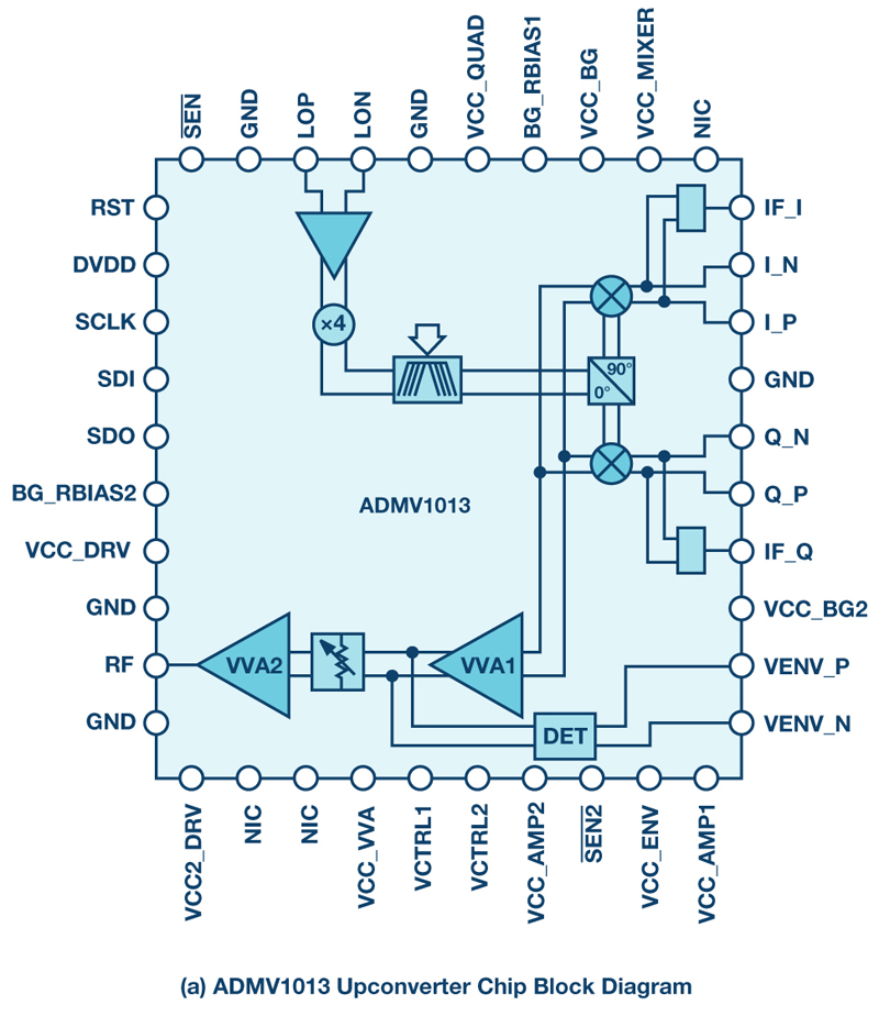
Figure 1a: The ADMV1013 upconverter chip block diagram
24 GHz to 44 GHz Wideband Integrated Upconverters and Downconverters Boost Microwave Radio Performance While Reducing Size
Analog Devices launched a pair of highly integrated microwave upconverter and downconverter chips, the ADMV1013 and the ADMV1014, respectively. These ICs operate over a very wide frequency range with 50 Ωmatch from 24 GHz up to 44 GHz and can support more than 1 GHzinstantaneous bandwidth. Performance attributes of the ADMV1013 and ADMV1014 ease the design and implementation of small 5G millimeter wave (mmW) platforms that cover the popular 28 GHz and 39 GHz bands in backhaul and fronthaul, as well as many other ultrawide bandwidth transmitter and receiver applications.
Each upconverter and downconverter chip is highly integrated (see Figure 1), comprised of in phase (I) and quadrature phase (Q) mixers with on-chip quadrature phase-shifter configurable for direct conversion to/from the baseband (operable from dc to 6 GHz) or to/from an intermediate frequency (IF) that can operate from 800 MHz to 6 GHz. The upconverter RF output has an on-chip transmit driver amplifier with a voltage variable attenuator (VVA), while the downconverter’s RF input contains a low noise amplifier (LNA) and gain stage with a VVA. Both chips’ local oscillator (LO) chain consists of an integrated LO buffer, a frequency quadrupler, and a programmable band-pass filter. Most of the programmability and calibration functions are controlled via an SPI interface, making the ICs easily software configurable to a performance level that is unmatched.
Click image to enlarge
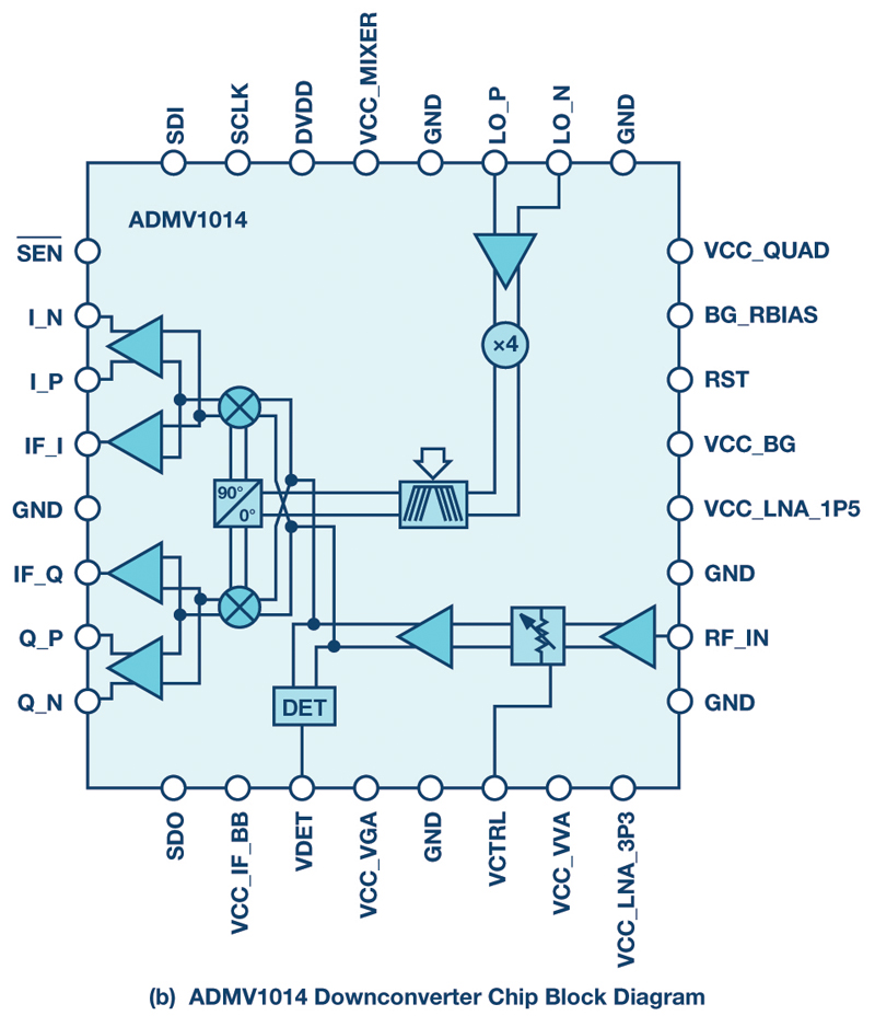
Figure 1b: The ADMV1014 downconverter chip block diagram
An Inside Look at the ADMV1013 Upconverter
The ADMV1013 offers two modes of frequency translation. One mode is direct up conversion from baseband I and Q to RF. In this I/Q mode, thebaseband I and Q differential inputs can accept signals from dc up to 6 GHz, for instance, generated from a pair of high speed transmit digital-to-analog converters (DACs). These inputs have a configurable common-mode range from 0 V to 2.6 V; thus, they can accommodate the interface requirements of most DACs. So when a DAC with a certain common-mode voltage is chosen, the upconverter’s registers can be easily set to match the optimum bias for that VCM voltage, simplifying the interface design. The other mode issingle-sideband upconversion to RF from complex IF inputs such as those signals generated by a quadrature digital upconverter device. Unique to the ADMV1013 is its capability to allow digital correction of the I and Q mixers’ dc offset error in the I/Q mode, resulting in improved LO leakage to the RF output. Achievable LO leakage after calibration can be as low as –45 dBm at the RF output, at maximum gain. An even more difficult challenge that plagues direct conversion radio design is that of I and Q phase imbalance, which gives rise to poor sideband suppression. An added challenge with direct conversion is that the sideband is usually too close to the microwave carrier that renders filters impractical. The ADMV1013 solves the problem by allowing users to digitally correct for the I and Q phase imbalance through register tuning. In normal operation, the upconverter exhibits an uncalibrated sideband suppression of 26 dBc. Using the on-chip registers, its sideband suppression can be improved to about 36 dBc after calibration. Both correction features are accessed via the SPI without extra circuitry. Additional suppression can be achieved by further adjusting the phase balance of the I and Q DACs at baseband, in the I/Q mode. These performance enhancement features minimize external filtering while improvingradio performance at microwave frequencies.
Click image to enlarge
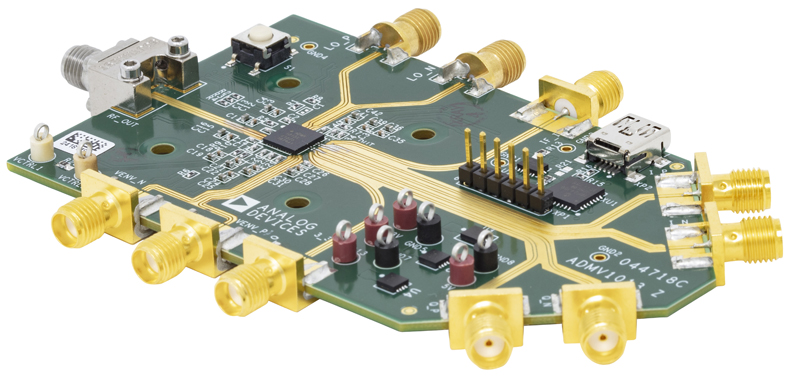
Figure 2: The ADMV1013 in a 6 mm × 6 mm surface-mount package shown on its evaluation board.
With the LO buffer integrated, the part requires only 0 dBm drive. Thus, the device can be conveniently driven directly from a synthesizer with integrated voltage controlled oscillator (VCO) like the ADF4372 or ADF5610, further reducing external components. The on-chip frequency quadrupler multiplies the LO frequency to the desired carrier frequency and is passed through a programmable band-pass filter to reduce the undesired multiplier harmonics prior to feeding the mixers’ quadrature phase generator stage. This arrangement greatly reduces spurious injection into the mixers while allowing the part to work with an external low cost, low frequency synthesizer/VCO. The modulated RF output is then amplified through a pair of amplifier stages with a VVA in between. The gain control provides a user adjustment range of 35 dB, with a maximum cascaded conversion gain of 23 dB. The ADMV1013 comes in a 40-lead land grid array package (see Figure 2). These features combine to provide exceptional performance, maximum flexibility, and ease of use, while requiring minimal external components. Hence, small microwave platforms can be realized such as small cell base stations.
An Inside Look at the ADMV1014 Downconverter
The ADMV1014 also has some of the similar elements such as the LO buffer, frequency quadrupler, programmable band-pass filter, and quadrature phase shifter in its LO path. However, architected as a down conversion device (see Figure 1b block diagram), the ADMV1014 has an LNA in its RF front end, followed by a VVA and an amplifier. A continuous 19 dB gain adjustment range is controlled by a dc voltage applied to the VCTRL pin. Users have the option to use the ADMV1014 in an I/Q mode as a direct conversion demodulator from microwave to baseband dc. In this mode, the demodulated I and Q signals are amplified at the respective I and Q differential outputs. Their gain and dc common-mode voltage can be set by registers via the SPI, allowing the differential signals to be dc coupled—for instance, to a pair of baseband analog-to-digital converters (ADCs). Alternatively, the ADMV1014 can be used as an image-reject downconverter to single-ended I and Q IF ports. In either mode, the I and Q phase and amplitude imbalance can be corrected via the SPI, improving the downconverter’s image rejection performance as it demodulates to baseband or IF. Overall, the downconverter provides a total cascaded noise figure of 5.5 dB, with a maximum conversion gain of 17 dB, over the frequency range from 24 GHz to 42 GHz. As the operating frequency gets close to the band edge, up to 44 GHz, the cascaded NF is still a respectable 6 dB.
Click image to enlarge
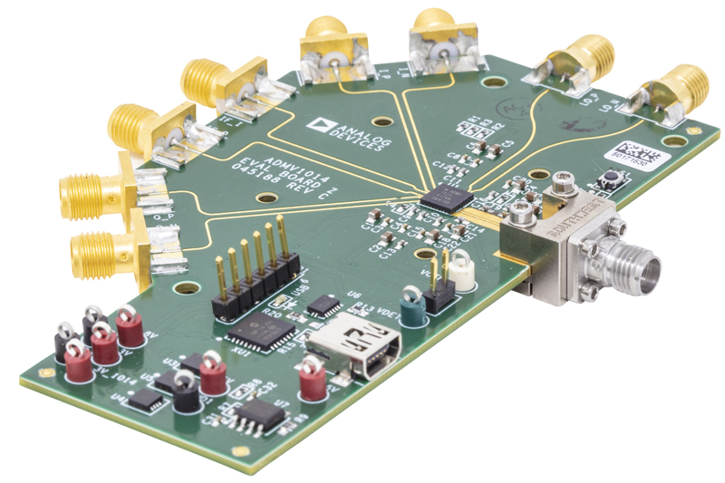
Figure 3: The ADMV1014 in a slightly smaller 5 mm × 5 mm package mounted on its evaluation board
Boosting 5G mmW Radio Performance
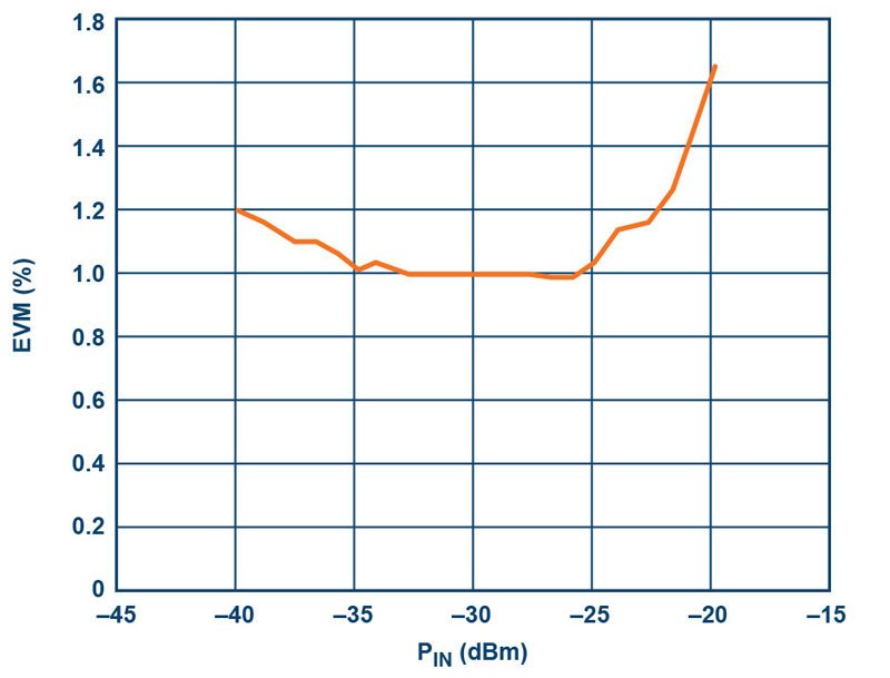
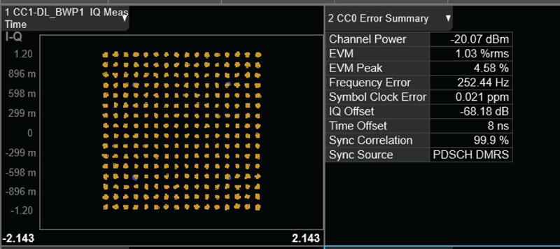
Figure 4 shows the measured performance of the downconverter at 28 GHzfrequency, using a 5G NR waveform over 4 independent 100 MHz channelsmodulated at 256 QAM at –20 dBm input power per channel. The resultingEVM measured –40 dB (1% rms), enabling demodulation of higher ordermodulation schemes that mmW 5G require. With the up and downconverter’s >1 GHz bandwidth capability, along with a 23 dBm OIP3 for theupconverter and 0 dBm IIP3 for the downconverter, the combination can beexpected to support high order QAM modulations—hence high data throughput. In addition, the devices benefit other applications such as satellite and Earth station broadband communication links, securedcommunication radios, RF test equipment, and radar systems. Their superior linearity and image rejection performance are compelling, and whencombined with compact solution size, small form factor, high performancemicrowave links, broadband base stations can be realized.
Click image to enlarge
Figures 4a & 4b: Measured EVM performance in rms percentage vs. input power and the corresponding 256 QAM constellation diagram at 28 GHz