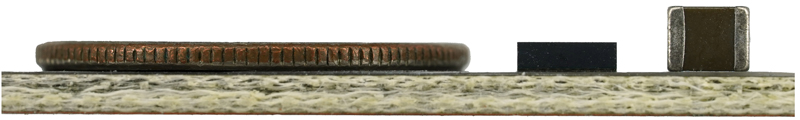
Figure 1. The small profile of the LTM4691 can be seen when placed next to a thin coin and a 1210-sized ceramic capacitor
3.6 V Input, Dual Output µModule Buck Regulator Produces 2 A per Channel in a 3 mm × 4 mm Footprint
The LTM4691 is a high efficiency, dual output step-down µModule buck regulator capable of 2A continuous output current for each channel from input voltages between 2.25 V and 3.6 V. This switch-mode power supply comes in a tiny 3 mm × 4 mm × 1.18 mm LGA package. This small footprint comprises the switching controller, power FETs, inductors, and all supporting components. Each output is independently resistor programmable from 0.5 V to 2.5 V.
The LTM4691 can deliver 2A per output with just a few small capacitors and resistors. The µModule regulator includes internal feedback loop compensation, reducing the number and size of additional components. The switching frequency defaults to 2 MHz without any external component or input, but it can be synchronized to a 1 MHz to 3 MHz external clock. To maximize the performance of the feedback loop, only a few small external capacitors need be added to complete the internally compensated loop — yielding sufficient stability margins and good transient performance. Other features include a PGOOD signal, output overvoltage protection, overtemperature protection, precision run thresholds, and output short-circuit protection.
Click image to enlarge
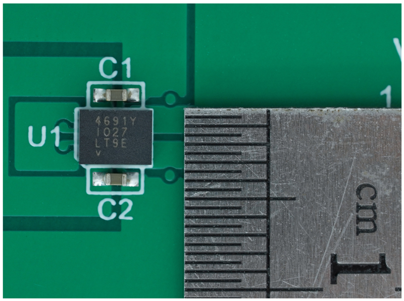
Figure 2. The small LTM4691 on the DC2910A demo board. Other than the two input capacitors shown, output voltage setting resistors and a couple capacitors populate the back of the board
Small Solution Using All-Ceramic Capacitors
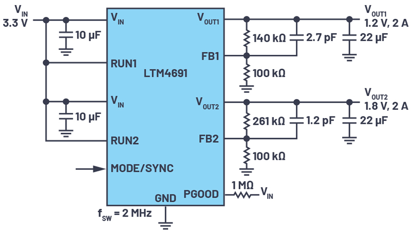
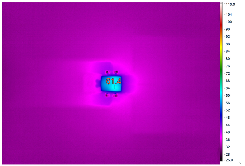
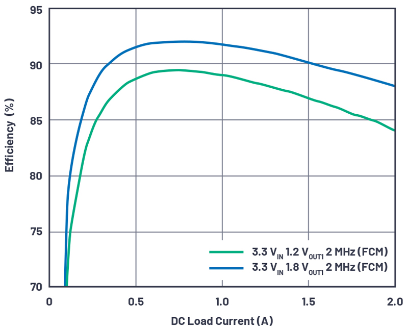
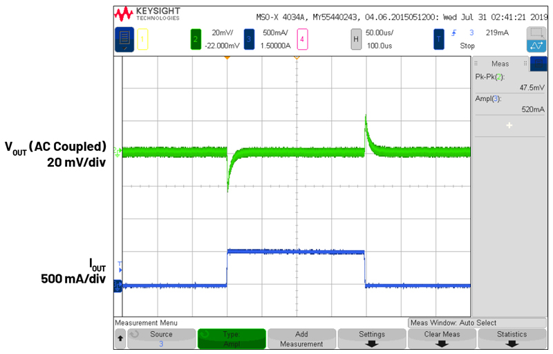
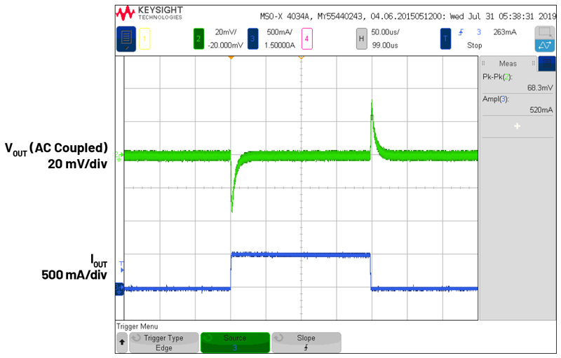
Figure 3 shows the scheme for a compact, all-ceramic capacitor solution, which takes maximum advantage of the internal circuitry of the LTM4691. Figure 2 shows a photo of the tiny solution. Figure 4, Figure 5, Figure 6, and Figure 7 show the thermal performance, efficiency, and load step performance for a DC2910A demo board.
Click image to enlarge
Figure 3. A simplified schematic for the LTM4691 setup for VIN = 3.3 V, VOUT1 =1.2 V, VOUT2=1.8V, and fSW = 2MHz
Click image to enlarge
Figure 4. LTM4691 VIN=3.3V, VOUT1 = 1.2 V, VOUT2 =1.8V, fSW = 2MHz, IOUT1 = 2A, IOUT2 = 2A, and Ta=23°C, with no forced airflow
Click image to enlarge
Figure 5. LTM4691 VIN = 3.3 V, VOUT1 = 1.2 V, VOUT2 = 1.8 V, and fSW = 2 MHz efficiency curves
Click image to enlarge
Figure 6. Loadstep at VIN =3.3 V, VOUT=1.2V, and fSW = 2MHz
Click image to enlarge
Figure 7. Loadstep at VIN=3.3V, VOUT=1.8V, and fSW = 2MHz
Conclusion
The LTM4691’s compact footprint and low profile enable it to fit tight spaces. Arguably just as important for compact designs: the LTM4691’s thermal performance and efficiency are high, minimizing the need for bulky thermal mitigation components. Likewise, transient performance and output stability are not sacrificed to fit the tiny package.