Author:
Akio Yamano, Misaki Takahashi, Hiroaki Ichikawa - Edited by Jeff Knapp, Fuji Electric America
Date
11/28/2017
 PDF
PDF
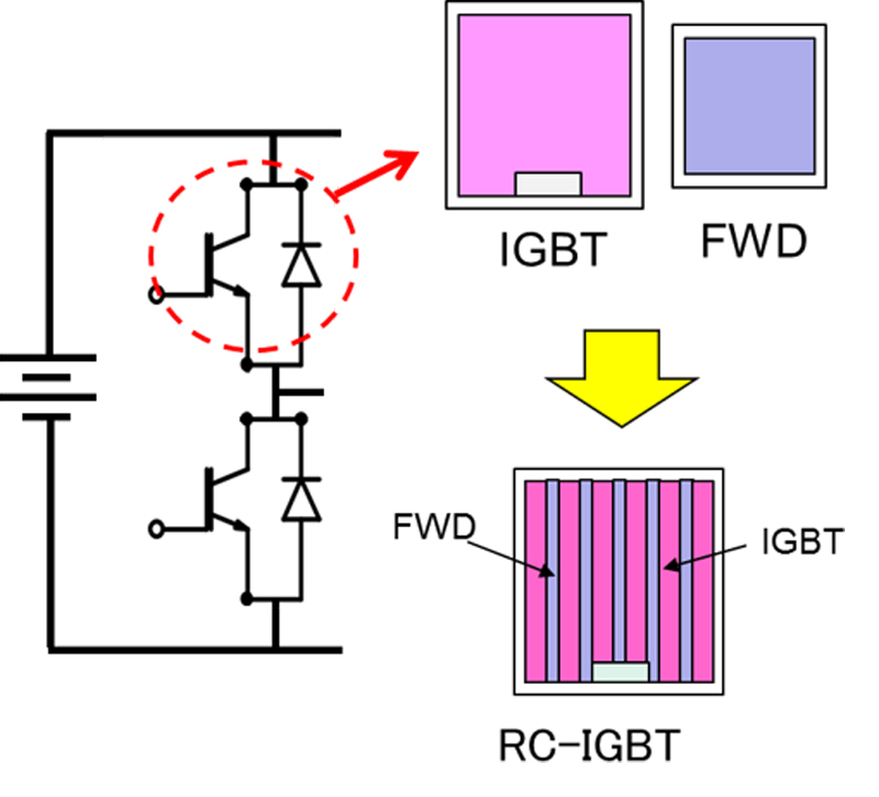
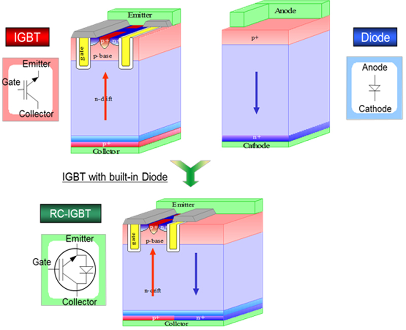
Figure 1. X Series RC-IGBTs
Ever since it commercialized insulated gate bipolar transistor (IGBT) modules in 1988, Fuji Electric has contributed to miniaturization, cost reduction, and performance improvement of power conversion equipment. It has done so through many technology innovations to miniaturize, reduce loss and improve the reliability of IGBT modules. However, any further miniaturization of IGBT modules increases power density, which may lead to lower reliability due to an increase in operating temperatures of IGBTs and free-wheeling diodes (FWDs). Accordingly, to miniaturize IGBT modules while maintaining high reliability, technology innovation of chips and packages is essential.
Fuji Electric has carried out technology innovation of chips and packages to commercialize the 7th-generation “X Series” IGBT module(1)(2). In addition, we have developed a reverse-conducting IGBT (RC-IGBT), which integrates an IGBT and a FWD into one chip, and in turn the 7th-generation “X Series” RC-IGBT module for industrial use that incorporates the chip(3)(4). By applying the chip technology of the 7th-generation X Series to optimize the chip structure, we have successfully reduced the number of chips and the total chip area. At the same time, we have maintained the same generated loss as that of a combination of the X Series IGBT and X Series FWD. Furthermore, by combining the package technology of the 7th-generation X Series with the RC-IGBT, we have reduced thermal resistance and improved reliability. These technology innovations have led to a further power density increase and miniaturization of IGBT modules, which were impossible through conventional combination of IGBT and FWD.
2. Features
2.1 Features of the “X Series” RC-IGBT for industrial applications
With a conventional IGBT, a current is run only in the direction from the collector to the emitter by applying a voltage to the gate. An inductor, which is used as a load of inverters widely in use as power conversion equipment, generates induced electromotive force in the direction to prevent any current change caused by the self-induction effect. Accordingly, the current has a behavior of flowing in the same direction even if the IGBT is turned off, and running a current in the reverse direction required an FWD to be connected in antiparallel with the IGBT. Meanwhile, the “X Series” RC-IGBTs for industrial applications (X Series RC-IGBTs) achieve the same purpose with one element by using an RC-IGBT (see Figure 1).
Figure 2 shows a cross-section view of the X Series RC-IGBT. The X Series RC-IGBTs apply the chip technology of the 7th-generation X Series IGBTs and use a trench gate as the surface structure and a field stop (FS) layer as the back structure. As with the X Series IGBTs, the X Series RC-IGBTs have employed even smaller design rules as compared with the 6th-generation “V Series” IGBTs and optimized the surface structure. In this way, they have achieved a significant reduction of the collector-emitter saturation voltage VCE(sat) that contributes to conduction loss. The latest thin wafer processing technology has also been applied to improve the trade-off relationship between the saturation voltage and turn-off switching loss. The X Series RC-IGBTs integrate FWD regions and have p-n junctions on the collector side. Accordingly, we have added the processes of patterning and impurity layer formation on the back to form the p-type layer on the collector side of the IGBT and the n-type layer on the cathode side of the FWD on the back of the same chip. In addition, the trade-off relationship has been improved by lifetime control.
Click image to enlarge
Figure 2. Cross-section view of the X Series RC-IGBT
2.2 Electrical characteristics
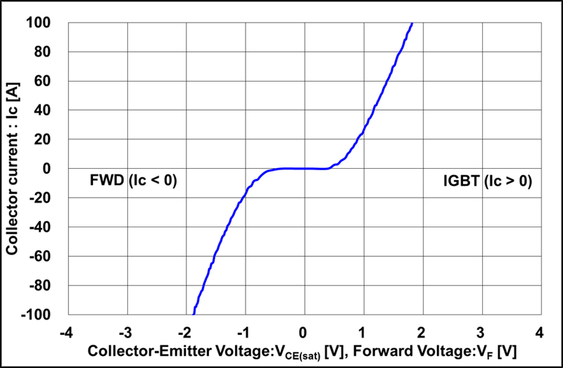
Figure 3 shows the output characteristic of the 1,200 V X Series RC-IGBTs. The X Series RC-IGBTs are capable of outputting a current in both the forward direction (IGBT) and reverse direction (FWD) with one chip. A saturation voltage lower than that of the V Series IGBTs has been realized by applying the chip technology of the 7th-generation X Series. With RC-IGBTs, electrons are injected into the cathode layer of the FWD region. This suppresses hole injection from the collector layer of the IGBT and thus hinders conductivity modulation. For that reason, snapback has been reported to occur (5)(6) in the low saturation voltage region. Meanwhile, with the X Series RC-IGBTs, snapback has been solved by optimizing the individual structures of the chip.
Click image to enlarge
Figure 3. Output characteristic of the 1,200 V X Series RC-IGBTs
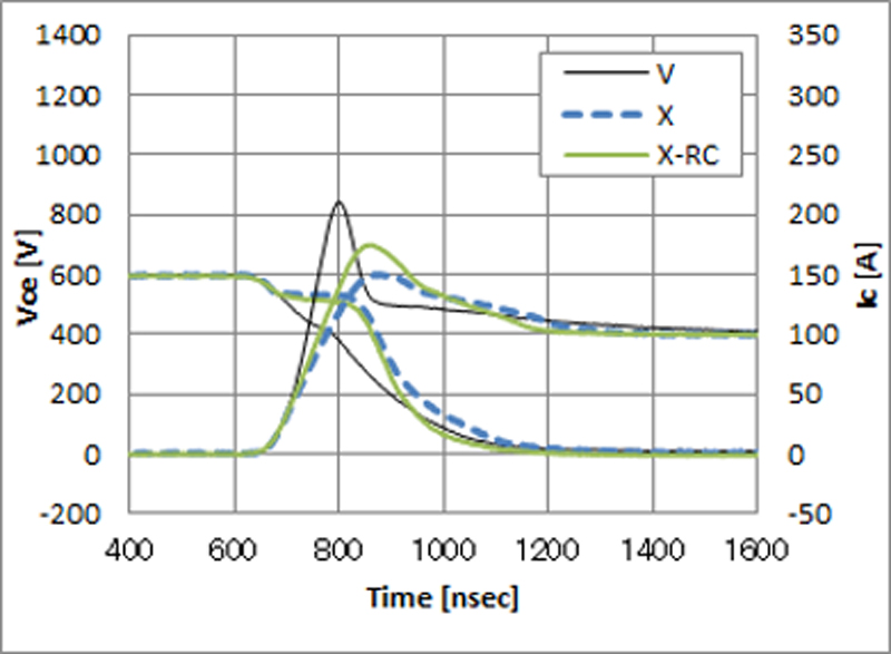
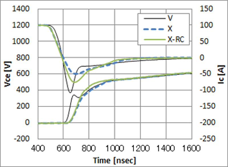
Turn-off waveforms of the X Series RC-IGBTs are shown in Figure 4, turn-on waveforms in Figure 5 and reverse recovery waveforms in Fig. 6. Figure 4 indicates that the surge voltage of the X Series RC-IGBTs is equivalent to that of combinations of the V Series IGBT and V Series FWD and of the X Series IGBT and X Series FWD. The tail current is smaller than that of the combination of the V Series IGBT and V Series FWD and the turn-off loss Eoff is lower by 23% with no abnormal waveforms observed. The X Series RC-IGBTs use a thinner wafer than that of the combination of the V Series IGBT and V Series FWD in order to improve the characteristics. Use of a thin wafer poses an issue of oscillation at turn-off and withstanding voltage degradation. However, with the X Series RC-IGBTs, the specific resistance and the individual structures have been optimized to successfully minimize oscillation and withstand voltage degradation. As shown in Figure 5 and Figure 6, the current waveforms for the combination of the V Series IGBT and V Series FWD have steep slopes but the X Series RC-IGBT realizes gentler current waveforms by optimizing lifetime control. Lowering the reverse recovery current peak Irrm and the tail current has reduced the reverse recovery loss Err by 20%.

Click image to enlarge
Figure 4. Turn-off waveforms of the X Series RC-IGBTs
Click image to enlarge
Figure 5. Turn-on waveforms of the X Series RC-IGBTs
Click image to enlarge
Figure 6. Current waveforms for the combination of the V Series IGBT
2.3 Thermal characteristics
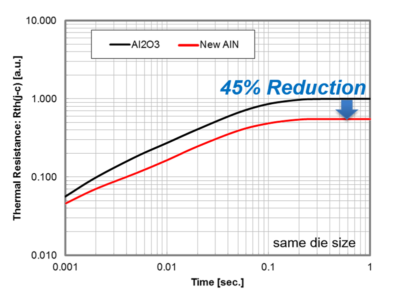
With the X Series RC-IGBTs, an IGBT and an FWD has been integrated into one chip and the heat produced due to generated loss in the IGBT or FWD regions is radiated from the entire chip. Accordingly, reduction of thermal resistance can be expected. To further reduce thermal resistance, a new aluminum nitride (AlN) insulating substrate has been employed as the package technology of the 7th-generation X Series.
The junction-case thermal resistance is shown in Figure 7. The new AlN insulating substrate features approximately 45% lower thermal resistance as compared with Al2O3 insulating substrates based on the same chip size, which is a significant improvement. This has resolved the issue of a temperature rise caused by miniaturization of IGBT modules. Furthermore, by optimizing wire bonding and employing high-strength solder and high-thermostability silicone gel, high reliability has been ensured and while guaranteeing continuous operation at 175°C.
Click image to enlarge
Figure 7. Junction-case thermal resistance
3. Power Density Increase and Miniaturization
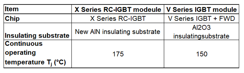
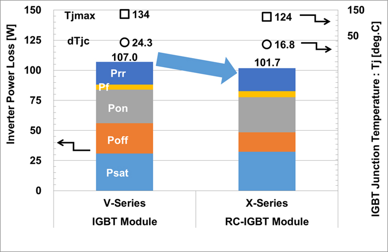
Table 1 shows a comparison with the V Series IGBT module of 1,200 V/100 A and Figure 8 shows calculation results of the power loss, junction temperature, Tj and junction temperature variation ΔTjc for the respective modules. By applying the chip technology and package technology of the 7th-generation X Series, we have significantly reduced the power loss and thermal resistance as compared with the conventional combination of the V Series IGBT and V Series FWD. We have thus ensured high reliability and guaranteed continuous operation at 175 °C. In addition, use of the X Series RC- IGBT makes it possible to reduce the number of chips and the total chip area, and miniaturization of IGBT modules can be expected. Based on these merits, applying the RC-IGBT chip technology and the chip technology and package technology of the 7th-generation X Series can produce a larger rated current than that of a conventional combination of IGBT and FWD with the same package.
Click image to enlarge
Table 1. Comparison with the V Series IGBT module of 1,200 V/100 A

Click image to enlarge
Figure 8. Calculation results of the power loss, junction temperature
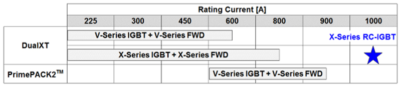
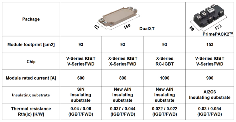
Table 2 illustrates Dual XT and PrimePACK2* as lines of products with a rated voltage of 1,200 V and Table 3 their features. Dual XT with a rated voltage of 1,200 V has the upper limit the rated current of 600 A for a combination of the V Series IGBT and V Series FWD. Through the use of the chip technology and package technology of the 7th-generation X Series, the rated current has been increased to 800 A by combining the X Series IGBT and X Series FWD. Furthermore, adopting the X Series RC-IGBT provides a module with a rated current of 1,000 A using the same package. In comparison to PrimePACK2 that uses the V Series IGBT and V Series FWD, Dual XT offers a 40% reduction in the module footprint. And, by using the X Series RC-IGBT, thermal resistance Rth(jc) can be reduced by 27%. In this way, it covers the range of PrimePACK2, which uses the conventional V Series IGBT and V Series FWD.
Click image to enlarge
Table 2. Dual XT and PrimePACK2* as lines of products with a rated voltage of 1,200 V
Click image to enlarge
Table 3. Dual XT and PrimePACK2* Features
Figure 9 shows the calculation results of output current Io in inverter operation and the maximum IGBT junction temperature Tjmax for the Dual XT products respectively with a combination of the V Series IGBT and V Series FWD, combination of the X Series IGBT and X Series FWD and the X Series RC-IGBT. In addition, using the X Series RC-IGBT can reduce power loss and the junction-case thermal resistance.By applying the package technology of the 7th-generation X Series, the guaranteed continuous operating temperature has been increased from the conventional 150 °C to 175 °C. As a result, a higher current density than before has been achieved with the same package and even higher power density and miniaturization of IGBT modules. In this way, it is possible to meet the requirements expected of IGBT modules such as miniaturization, loss reduction and higher reliability. In the future, we intend to continue working on technology innovation of IGBT modules and contribute to the realization of a sustainable society with improved energy management.
Click image to enlarge
Figure 9. Calculation results of output current Io in inverter operation
References
1) Kawabata, J. et al. “The New High Power Density 7th Generation IGBT Module for Compact Power Conversion Systems” Proceeding of PCIM Europe 2015.
2) Kawabata, J . et al. 7th-Generation “X Series" IGBT Module. FUJI ELECTRIC REVIEW. 2015, vol.61 no.4
p.237-241.
3) Takahashi M. et al. “Extended Power Rating of 1200 V IGBT Module with 7 G RC- IGBT Chip Technologies”, Proceeding of PCIM Europe 2016.
4) Takahashi K. et al. “1200 V Class Reverse Conducing IGBT Optimized for Hard Switching Inverter”, Proceeding of PCIM Europe 2014.
5) Takahashi H. et al. “1200 V Reverse Conducting IGBT” Proceeding of ISPSD 2004. p.133-136.
6) M. Rahimo. et al. “The Bi-mode Insulated Gate Transistor (BlGT) A Potential Technology for Higher Power Applications”, Proceeding of ISPSD 2009. p.283-286.
Note* PrimePACK: A registered trademark of Infineon Technologies AG, Germany.