Ryan Manack from iDEAL Semiconductor tells PSD how the company's innovation ends the need for cost/performance trade-offs in silicon MOSFET designs
Mark Twain has been rumoured to have once said that “rumours of his death have been greatly exaggerated". The same could be said for silicon in power designs. For almost a decade now, proponents of GaN and SiC technologies have been telling us that it is only a matter of time until we see the end of silicon. However, silicon solutions not only refuse to lay down and die, but continue to thrive. There are four good reasons for that – silicon is cheap, it is easy to design in, it is very robust, and, finally, some clever people are still working to get every last drop of value from the material. The latest of these innovators is iDEAL Semiconductor, who have just announced a range of devices with a new structure, which the company claims will increase performance while lowering the cost of silicon power devices.
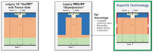
Fundamental changes in silicon transistor design don’t happen often, but when they do they always breathe new life into the industry. Over the past few decades, there have been two major changes. Initially, in 1979 International Rectifier developed HexFET technology, which effectively replaced BJTs in a lot of applications. HexFETs were a big step forward for performance and efficiency, but started to lose a bit of steam as voltages increased. As the structure resistance grew with breakdown voltage, it was difficult to lower resistance at higher voltages.
The next big advance came in the late 1990s, when Infineon launched superjunction technology, a power MOSFET architecture that included a p-region which reshaped the electric field inside of the device, dramatically lowering resistance. The company is now in its eighth generation of superjunction devices, and according to Ryan Manack, Vice President of Systems, Applications and Marketing at iDEAL Semiconductor, its performance has now started to plateau and the technology is reaching the limits of manufacturing. He explains that the performance plateau is due to the structure’s p-regions not contributing directly to conduction, only to voltage blocking. Additionally, to get higher performance requires more processing time and additional mask layers which makes each new generation of the technology more time consuming and expensive.
The new SuperQ technology developed by iDEAL Semiconductor takes a step back in time to use the basic structure of HexFET technology with improvements that remove its downsides. Manack expands, “SuperQ looks a lot like the HexFET structure with its full conduction region open. The main difference is that we use a charge compensation principle similar to superjunction, but instead of a p-region, we use a thin film on the side walls to reshape the electric field. The thin film itself is commonly used in solar panel manufacturing. The new structure can block voltage effectively, while opening up the conduction region. The end result is a high-performance device that provides lower resistance and reduced switching losses. In addition, its ease of manufacture means that there is no need to trade off cost and performance.”
The company has launched a 150V MOSFET with a resistance of 6.4 mΩ in a 5 x 6 mm PDFN package. A 200V device is currently sampling in TOLL, TO-220, D2PAK-7L and PDFN packages, and 300V and 400V versions are in the works, with Manack estimating that the technology could scale to 700V and possibly higher. He claims that one big difference between SuperQ and competing technologies is that the same structure can be used going up voltage levels. He explains, “300V to 400V has been a dead zone from a technology perspective. Traditional 150V power devices differ from 600V technologies in their construction, while ours is exactly the same. At the 400V level, we compared ourselves to a recently released SiC device from a competitor, and our structure delivers similar performance with an even lower resistance. Our switching charge is 2.1 times lower than the same competitor, and lower than three leading silicon suppliers. This means designers can switch faster for the same losses, or keep the same switching frequency for lower losses. From a performance standpoint, we are excited that our entry point is the same or better than market leading solutions, and we are confident that there is a lot of scope for improvement in the future generations of SuperQ technology.”
As for applications, Manack says that there are areas where SuperQ technology naturally excels, “with a rugged and robust silicon structure, very low RDS on and a high current rating, SuperQ devices are ideal for withstanding the tremendously high currents that flow through BLDC motors in a locking event, giving the controller time to sense the short and stop the operation. This allows a reduction in the number of parallel MOSFETs required, reducing system cost, along with the traditional benefits gained from low switching losses. We are working with AI data center customers, also to reduce the number of MOSFETs needed to work with their 54V intermediate bus. Our new 150V and 200V products form the basis of very good synchronous rectifiers in these systems and we have a lot of test data to prove it. In general applications, we have found a reduction in power losses and increased efficiency, and that leads to reduced operating temperatures. In one telecom networking application, customer tests showed a seven degree difference between a SuperQ device and a competitor. This allows customers to push power higher, or simplify their thermal management.”
Although the new SuperQ technology is debuting in MOSFETs, Manack says there is potential to expand its use into IGBTs, diodes, other power ICs, and even future semiconductor materials.
https://idealsemi.com/wp-content/uploads/2025/07/iDEAL-Whitepaper-D4-2.pdf

.jpg)