A Look at the Advantages of 4th Generation SiC MOSFETs
Design Advancements and Applicational Benefits
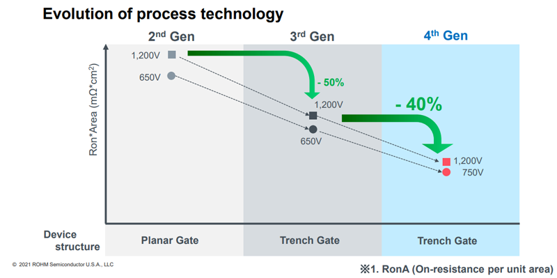
Figure 1: The evolution of process technologies improves upon the trench gate structure for a lowered on-resistance per unit area
Power is arguably the most critical part of next-generation electric vehicles, alternative energy systems, and data centers, and industrial power supplies are increasingly reliant on efficient operations to save on energy costs and increase the effectiveness of their subsystems/equipment. In these applications, even a marginal improvement in efficiency can yield massive power savings ― and in the case of EVs, lessen charge time. A total of 4.7 terawatt hours were attributed to EV charging in the United State alone in 2020. If the various on-board chargers (OBCs) and DC charging systems exhibited even a 1% improvement in efficiency, there would be a total of 47 gigawatt hours of power saved nationwide ― a number that is far from negligible. And, given that EVs, alternative energy, and power supplies for large-scale facilities are only trending upwards, the energy savings will be greater.
All of these highly desirable power device characteristics have led to an increase in demand for SiC MOSFETs in many applications across the power spectrum. As such, fabrication facilities and design houses are meeting these demands with newer process technologies and package enhancements. ROHM’s 4th generation of SiC MOSFETs reduces the on-resistance per unit area (RonA) by 40% over 3rd generation SiC MOSFETs without sacrificing short circuit withstand time. This achieves lower power losses and a much higher efficiency than previous generations of SiC MOSFETs. The combination of the lowered on-resistance and high switching frequencies enables both a high degree of miniaturization and a lowered power consumption ― two parameters that are highly desirable in modern power electronics applications.
This article dives into the evolution of SiC MOSFETs and how ROHM has been able to achieve best-in-class on-resistance per unit area by iteratively improving their process in-house. It provides heuristics for designers looking to switch from 3rd- to 4th-generation devices and examines the applicational advantages of 4th generation SiC MOSFETs.
4th Generation SiC MOSFET ― a technology overview
A process evolution for 4th Gen SiC MOSFETs
The 4th generation of SiC MOSFETs have a further improvement on the double-trench structure allowing for a more substantial drop in on-resistance and input capacitance (Figure 1). In the process of continually improving on RonA device designers will face the trade-off of a shorter short-circuit withstand time (SCWT) ― the time it takes for MOSFET to fail due to a short circuit. The 4th generation SiC MOSFETs, however, do not sacrifice on short circuit withstand time and therefore enable converter and power supply designs with greater efficiency, smaller packaging, and a high reliability in the field.
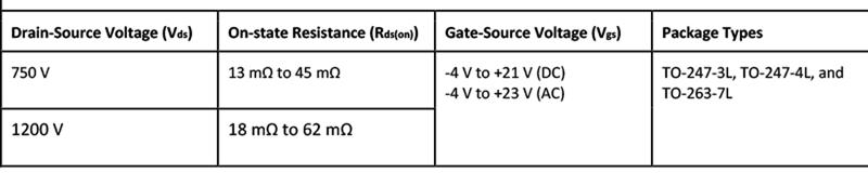
Basic specifications
The 4th generation of SiC MOSFETs include high drain-source voltages (Vds) of 750 V or 1200 V, on-state resistances (Rds(on)) ranging from 13 mΩ to 62 mΩ, and an easy drive with gate-source voltages (Vgs) ranging from -4V up to +23V (Table 1). The major benefits of these device-level improvements yield:
● Low power loss designs
● User friendly implementations
● High device reliability
Click image to enlarge
Table 1: Specifications for ROHM’s 4th Generation SiC MOSFETs
Low power loss designs
Lower conduction losses
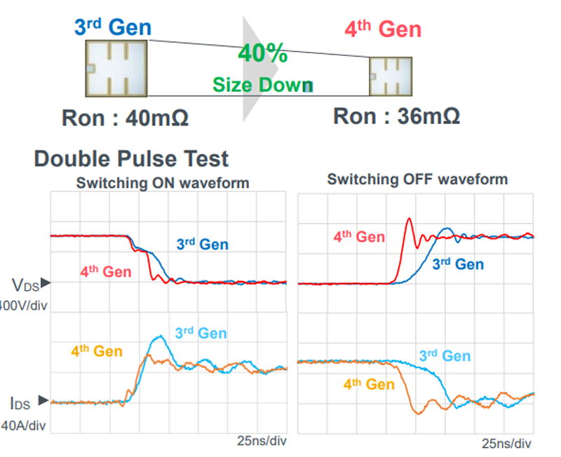
Reducing the on-resistance (Ron) allows designers to readily achieve a reduction in both conduction and switching losses. For a chip with the equivalent chip size, the on-resistance 3rd generation of SiC MOSFETs was 60 mΩ; this improved to 36 mΩ with the 4th generation. The 57% reduction in on-resistance directly impacts conduction losses that are caused by the on-resistance of the drain-source channel.
Buck converters using the equivalent chip size for a 4th generation SiC MOSFET over the 3rd generation will see a considerable reduction in conduction losses. Figure 2 illustrates this reduction by comparing the efficiency of two buck converters: one with the 3rd gen MOSFETS and the other with 4th gen MOSFETs. There is significantly less heat generation in the newer generation of MOSFETs for the same output power, which leads to a 53% improvement in conduction losses.

Click image to enlarge
Figure 2: The cutting of conduction losses leads to a reduction in heat generation. These devices are able to operate much more efficiently with the same output power
Reduction in switching losses
The 4th generation of SiC MOSFETs also exhibit a reduction in parasitic capacitance for the same chip size ― parameters that directly impact switching losses. The input capacitance (Ciss) is decreased along with the output capacitance (Coss) that is reduced by 15% and reverse transfer capacitance (Crss) cut down by 90%. As shown in Figure 3, this optimizes for on- and off-loss where the switching waveforms show much sharper rise and fall times. The lowered gate-drain capacitance (Crss) enables much faster switching while the significantly lowered Crss and Ciss ratio (Crss/Ciss) avoids self turn-on. This is due to the fact that transient gate current flows through Crss to the gate resistance, which raises the gate voltage and causes turn-on.
Click image to enlarge
Figure 3: Switching losses are significantly cut in the 4th generation of SiC MOSFETs while all parasitic capacitances are reduced allowing for a smaller device size
ROHM’s improvement on the double trench technology directly results in a more efficient device operating at higher switching frequencies. These factors also enable a large degree of miniaturization where converter and power supply designs require smaller heatsinks and peripherals (e.g., gate drivers, passives, magnetics, etc). The improvement in efficiency resulted in a 40% decrease in the heatsink volume, saving on size, weight, and cost of the design for the same power output.
Key benefits for users of switching to 4th-generation SiC MOSFETS
Optimization of gate drive circuitry
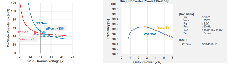
It is important to optimize the gate drive circuitry, as it has a significant effect on the losses of the devices. This is a necessary step in order to fully realize the high-speed switching characteristics of SiC devices. Typically, the recommended positive gate drive voltage is between 15 V and 18 V where the on-resistance varies by only 7% from the 3rd generation of SiC MOSFETs (Figure 4). In a buck converter design, there is no significant difference in conversion efficiency between these gate voltages in a light load condition. For heavy loads however, 18 V voltage exhibits a marginally higher efficiency. This allows the 4th generation of SiC MOSFETs to be a drop-in replacement for current 3rd generation SiC designs.
Click image to enlarge
Figure 4: The recommended gate drive voltage for the 4th generation of SiC MOSFETs stands between 15V and 18V where there are no significant differences in on-resistance and efficiency
Shedding the negative bias circuit
The 4th generation of SiC MOSFETs feature a high gate threshold voltage (Vth). This avoids self turn-on of the low-size MOSFET bridge circuit topologies even at high temperatures. The reason for this is due to the fact that self turn-on occurs as a result of fluctuations in the gate voltage (Vgs) through Cdg and Cgs during a steep change in Vds. When the Vgs exceeds the Vth, the low side MOSFET in the bridge circuit can accidentally be turned on. The high gate threshold voltage allows these devices to operate more safely in these very common circuit topologies where the positive Vgs surge will not exceed Vth (Figure 5). Without the negative bias, the design engineer is able to simplify the gate driver power supply circuit design and shed the entire negative bias circuit.

Click image to enlarge
Figure 5: The high gate threshold voltage of 2.8V avoids the common failure mode of self turn-on that can occur during gate voltage spikes induced by voltage transients dVDS/dt
An increased design tolerance when gate resistance values
One common method to mitigate the negative effects of di/dt and dVDS/dt in power devices is by increasing the value of the gate resistance (RG). However, tuning this value can directly increase switching losses and negatively impact design efficiency. The reduction of the internal gate resistance (RG_INT) allows for a more flexible external gate resistance (RG_EXT) value. This is due to the fact the total gate resistance (RG) is the sum of the internal and external gate resistances (RG_INT+RG_EXT). When comparing the 3rd generation to the 4th generation of SiC MOSFETs, if the external gate resistance value is kept identical, the switching losses are still smaller by comparison. This allows a great degree of flexibility in choosing an ideal RG for the design.

Click image to enlarge
Figure 6: Design example when the VDS surge is 580V
High device reliability through a longer SCWT
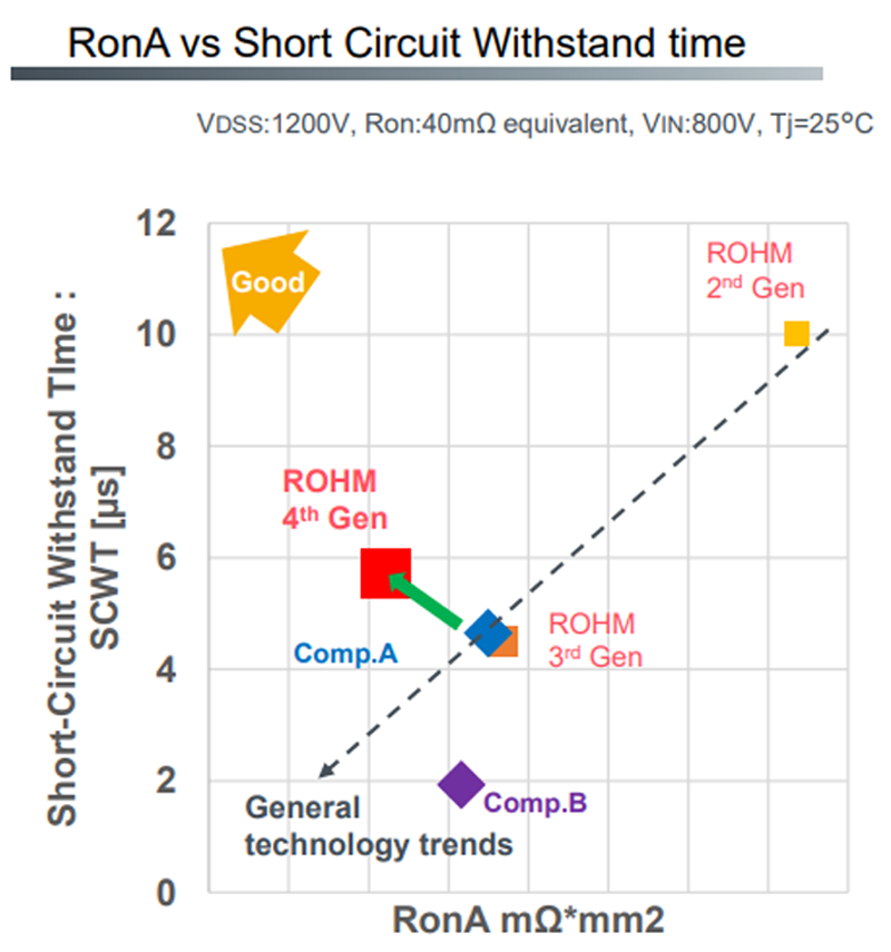
As stated earlier, the unique device structure improves on the trade-off between the on-state resistance per unit area (RonA) and short circuit withstand time (SCWT). The general technology trend illustrates a noticeable line where most power devices fall (Figure 7). Typically, the bigger RonA, the longer the SCWT and the smaller RonA, the shorter the SCWT. This is due to the fact that the saturation current generally rises when RonA decreases. When saturation current rises, so does short circuit current resulting in a shorter SCWT. However, the 4th gen MOSFETs fall outside this line and manage to improve on both RonA and SCWT over the 3rd gen of MOSETs as well as competitive brands. This improvement is realized by reducing the saturation current in the 4th gen MOSFETs.
Click image to enlarge
Figure 7: RonA versus short-circuit withstand time (SCWT)
Conclusion
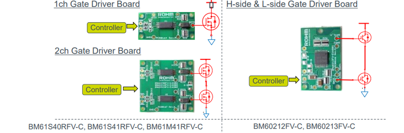
ROHM provides numerous evaluation boards and simulation models to speed up design and prototyping with the 4th generation MOSFET. These include the following:
- 1 channel gate driver board
- 2 channel gate driver board
- H-side and L-side gate driver board
- Half-bridge drive evaluation board
The first three driver boards are miniaturized so that they can easily connect to the power device on the customer’s board to be evaluated (Figure 8). The half-bridge drive evaluation board enables a double pulse test up to 250 A, up to 500 kHz of switching operation and various power supply topologies including buck, boost, and half-bridge. These evaluation boards speed up the design and development process for a quicker time-to-market (TTM).
Click image to enlarge
Figure 8: Gate driver boards can be connected to the power device and easily evaluated with a simulation model provided
ROHM’s 4th generation of SiC MOSFETs features a significant improvement in on-state resistance, equating to a reduction in conduction losses. Both on and off losses (switching losses) are also improved upon with a reduction in parasitic capacitances. This yields a much more efficient end design with smaller power devices and passive sizes as well as a potential reduction in component count.
All of these factors combined cause the 4th generation of SiC MOSFETs to be a cutting-edge device on the market when compared to both ROHM’s older iteration of SiC devices, competitor SiC devices, and conventional Si-devices. Employing these components in mid- to high-powered applications with tight design tolerances and the need for high efficiency designs is highly desirable. Not only does it allow the product manufacturer to produce a more efficient, higher quality, and better performing product for less long term costs, but it also has the potential to decrease BOM costs outright through the use of simpler circuit topologies.