Integrated multiplexed-input ADC alleviates increased channel density and power dissipation challenges
Many applications in industrial, instrumentation, optical communication and healthcare industry use multi-channel data acquisition systems that result in increased printed circuit board (PCB) density and thermal power dissipation challenges. The need for increased channel density in these applications is driving the demand for high channel count, low power and compact form factors.
These applications also demand precision measurements, reliability, affordability, and portability. Maintaining balance among optimum performance, thermal stability, and PCB density is a constant challenge for them. Therefore, system designers are continually pressed to find innovative ways to tackle thermal power dissipation challenges while accommodating increased circuit density in a small PCB footprint while minimizing overall bill of material costs.
One means to address this focuses on a low power, integrated, multiplexed-input ADC solution to address these technical challenges for space-constrained applications such as coherent optical transceivers and other portable instruments. The proposed solution using an integrated multiplexed input 8-channel, 16-bit, 250kSPS PulSAR ADC AD7689 is available in a miniature, wafer-level, chip-scale package (WLCSP) footprint that saves over 60 percent board space, which addresses the challenges for increased channel density and battery-powered portable systems while offering flexible configuration and precision performance.
Coherent optical transceivers
The market for 100Gbps optical transceivers is uniquely positioned to grow in the next decade for high-speed coherent optical transmission. In optical networks, as bit rates per channel increases from 10Gbps towards 100Gbps and higher, the optical fiber non-idealities severely degrade signal quality and affect its transmission performance.
Technical challenges arise in long-haul optical networks when penalties occur in terms of optical noise, non-linear effects, and dispersion due to optical fiber impairment. To address these significant challenges, various manufacturers of 40G and 100Gbps optical transceivers use a coherent technology that allows higher data rate connectivity with maximum reach at longer distances for metro long haul, long-haul and ultra-long-haul networks. The coherent technology generally combines multi-level signal formats and coherent detection using dual polarization, quadrature, phase-shift keying (DP-QPSK) for optimized signal modulation, allowing immunity to fiber impairments at higher data rates and making 100Gbps transmission economically and technically feasible.
The next step
The next generation of 100Gbps (and above) data rate coherent optical transceivers will require lower power dissipation and miniature form factor to allow increased channel density for significant space, power and cost savings. Depending on requirements, the channel count varies anywhere from 8 to 32 in an optical system. The component placement and trace routing become prominent for the PCB designers, especially for high channel-density systems.
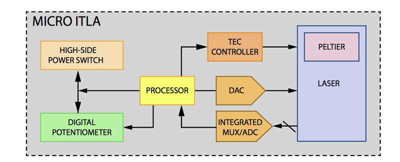
A simplified block diagram of a generic optical module is shown in Figure 1, which includes transmitter, receiver, micro-ITLA (integrated tunable laser assembly) and data acquisition components. Figure 2 shows the simplified block diagram of micro-ITLA, which is a wideband electronically tunable laser device and controls rapid wavelength switching. The transmitter includes Mach-Zehnder driver and modulator to control the amplitude or intensity of the exiting laser light. The multiplexed input ADC can be used in control and monitoring functions to digitize the data from the multiple channels in optical module and micro-ITLA.

Click image to enlarge
Figure 1. Simplified block diagram of optical module
Click image to enlarge
Figure 2. Simplified block diagram of micro integrated tunable laser assembly
The key challenge for optical transceiver systems is to acquire and process wider bandwidth signals or multiplex number of input channels at lower power in a smaller footprint. The size, power, and cost structure of today’s coherent transceivers originally designed for long-haul applications limit their utilization in more cost-sensitive metro networks. The metro networks include: metro regional 500km – 1000km, metro core 100km – 500km and metro access <100km applications. For metro networks, the space comes at a high premium, making line-card density very critical and consequently, a path to a lower-cost optical line cards or pluggable modules in a smaller footprint has become increasingly important for coherent applications.
Integrated multiplexed-input 8-channel, 16-bit, 250kSPS ADC
Manufactured on Analog Devices proprietary 0.5μm CMOS process, the AD7689 is a leading integrated multiplexed input 8-channel, 16-bit, 250kSPS SAR based ADC. A device such as this is ideally suited for increased channel density applications such as coherent optical transceivers and portable vital sign monitors and wearables. The integrated 8-channel low crosstalk multiplexer introduces minimal mismatch from between adjacent channels and allows sequential sampling. Figure 3 shows a simplified AD7689 block diagram for a multichannel data acquisition system, which offers easy to use flexible configuration options and precision performance.
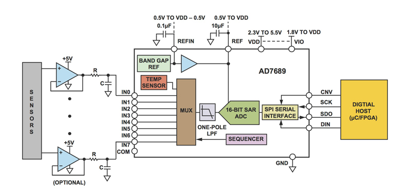
Click image to enlarge
Figure 3. AD7689 typical application diagram
For multichannel, multiplexed applications, some designers use a low-output-impedance buffer to handle the kickback from the multiplexer inputs depending on throughput rate used. The input bandwidths of the SAR ADC (tens of MHz) and ADC driver (tens to hundreds of MHz) are higher than the sampling frequency, whereas the desired input signal bandwidth is typically in the tens of Hz to hundreds of kHz range.
Therefore, depending on the system requirements, a single-pole, low-pass RC antialiasing filter may be required at the input of the multiplexer to eliminate unwanted signals (aliases) from folding back into the bandwidth of interest, to limit the noise and to reduce settling time issues. The value of the RC filter used at each input channel should be carefully selected based on the following trade-off because too much band limiting can affect settling time and increase distortion: if the capacitance is large, it will help attenuate the kickback from the multiplexer, but it can also make the previous amplifier stage unstable by degrading its phase margin.
C0G or NP0 type capacitors are recommended for an RC filter that has high Q, low temperature coefficient, and stable electrical characteristics under varying voltages. A reasonable value of series resistance should be chosen to keep the amplifier stable and limit its output current. The resistance cannot be too large, or the ADC driver will not be able to recharge the capacitor after the multiplexer kickback.
Precision performance
A device like the AD7689 allows the choice of a very low temperature drift internal voltage reference, an external reference, or an external buffered reference. The best SNR is achieved with a 5 V external reference, as the internal reference is limited to 4.096 V. For applications that require multiple devices, it is more effective to use the internal reference buffer to buffer the external reference voltage, thus reducing SAR conversion crosstalk.
The AD7689 includes a channel sequencer useful for scanning channels as singles or pairs, with its internal temperature sensor enabled or disabled in a repeated fashion. It offers a flexible serial digital interface compatible with SPI, MICROWIRE, QSPI, and other digital hosts. Its 14-bit internal configuration register allows the user to select various options including a number of channels to be sampled, reference, temperature sensor and channel sequencer.
The interface allows 4-wire read during conversion, read after conversion and read spanning conversion modes with and without busy indication. It offers an excellent SNR of ~93dB and THD of -102dB bits with a 5 V external reference for a 20 kHz input tone while running at the full speed of 250kSPS as shown in its FFT performance in Figure 4.
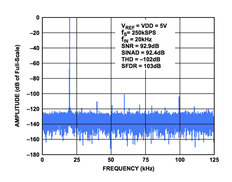
Click image to enlarge
Figure 4. AD7689 SNR, SINAD and ENOB versus Reference Voltage
Power dissipation
The AD7689 requires two supplies: an analog and digital core supply (VDD) and a digital input/output interface supply (VIO) for a direct interface with any logic between 1.8 V and VDD. The VDD and VIO pins can also be tied together to save on the number of supplies required in the system, and they are independent of power supply sequencing. Powered from +5 V (VDD) and +1.8 V (VIO) supplies, it enables very low power consumption typically around 12.5mW at 250kSPS with a 5V external reference as shown in Figure 5. It powers down automatically at the end of each conversion phase and consumes a typical standby current of only 50nA. Its power also scales linearly with throughput rate, making the ADC power efficient and well suited for both high and low sampling rates even as low as a few Hz and for portable and battery powered systems.
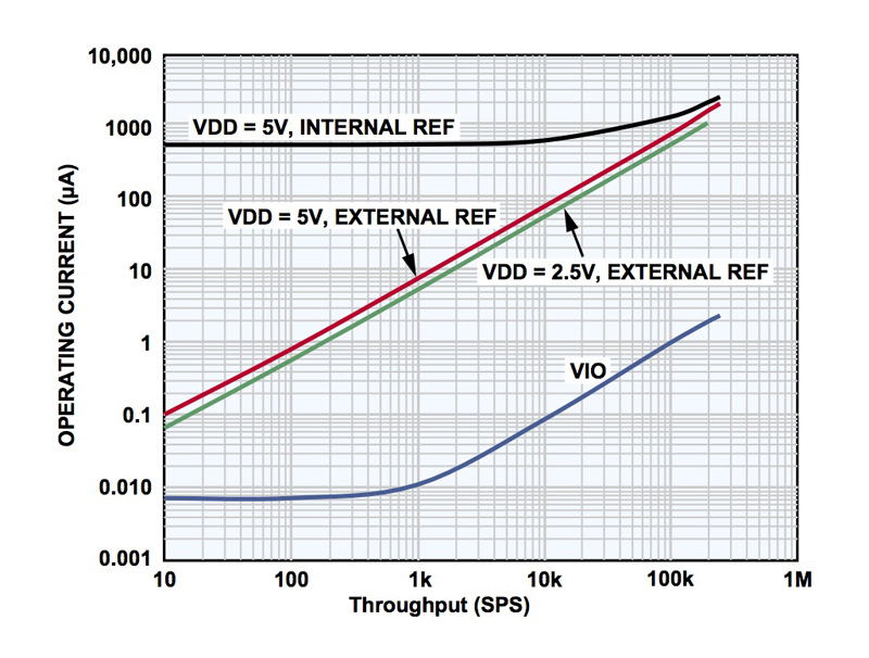
Click image to enlarge
Figure 5. AD7689 Operating current vs throughput
The AD7689 is now available in 2.39mm x 2.39mm pin-compatible wafer level chip scale package (WLCSP), which is a ~2.8x smaller form factor compared to its existing 4mm x 4mm lead frame chip scale package (LFCSP), allowing increased circuit density in a small system footprint. The Figure 6 compares a miniaturized size of its WLFSCP with a size of US Dime.

Click image to enlarge
Figure 6. Size Comparison of AD7689 Wafer Level Chip Scale Package with a dime
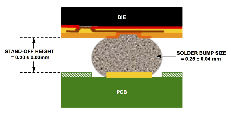
The active side of the of AD7689 WLCSP die is inverted and can be connected to the printed circuit board (PCB) using solder balls and its dimensions after PCB assembly are as shown in the Figure 7. The actual separation between the surface of the die and the substrate (stand-off) after PCB assembly varies with the amount of solder screen printed on to the substrate and pad diameter.
Click image to enlarge
Figure 7. AD7689 WLCSP dimensions after PCB assembly