press x to close
Author:
Institute of Industrial Science, The University of Tokyo
Date
04/01/2020
 PDF
PDF
The University of Tokyo researchers develop a machine-learning algorithm for detecting atomically thin 2D materials, including graphene, from a microscope image in a fraction of a second--which may accelerate the industrial-scale production of next-generation electronics
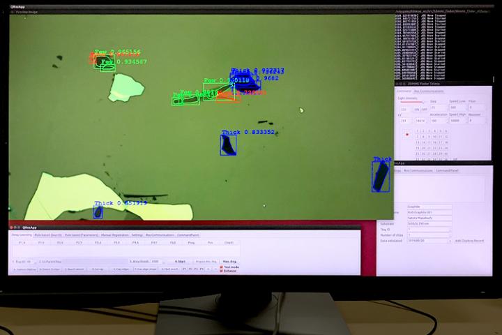
Researchers at the Institute of Industrial Science, a part of The University of Tokyo, demonstrated a novel artificial intelligence system that can find and label 2D materials in microscope images in the blink of an eye. This work can help shorten the time required for 2D material-based electronics to be ready for consumer devices.
Two-dimensional materials offer an exciting new platform for the creation of electronic devices, such as transistors and light-emitting diodes. The family of crystals that can be made just one atom thick include metals, semiconductors, and insulators. Many of these are stable under ambient conditions, and their properties often different significantly from those of their 3D counterparts. Even stacking a few layers together can alter the electronic characteristics to make them suitable for next-generation batteries, smartphone screens, detectors, and solar cells. And perhaps even more amazing: you can make some yourself using office supplies. The 2010 Nobel Prize in Physics was awarded for the realization that atomically thin "graphene" can be obtained by exfoliating piece of pencil lead, graphite, with a piece of sticky scotch tape.
So, what keeps you from making your own electronic devices at work between meetings? Unfortunately, the atomically thin 2D crystals have low fabrication yields and their optical contrasts comprise a very broad range, and finding them under a microscope is a tedious job.
Now, a team led by The University of Tokyo has succeeded in automating this task using machine learning. The used many labeled examples with various lighting to train the computer to detect the outline and thickness of the flakes without having to fine tune the microscope parameters. "By using machine learning instead of conventional rule-based detection algorithms, our system was robust to changing conditions," says first author Satoru Masubuchi.
The method is generalizable to many other 2D materials, sometimes without needing any addition data. In fact, the algorithm was able to detect tungsten diselenide and molybdenum diselenide flakes just by being trained with tungsten ditelluride examples. With the ability to determine, in less than 200 milliseconds, the location and thickness of the exfoliated samples, the system can be integrated with a motorized optical microscope.
"The automated searching and cataloging of 2D materials will allow researchers to test a large number of samples simply by exfoliating and running the automated algorithm," senior author Tomoki Machida says. "This will greatly speed the development cycle of new electronic devices based on 2D materials, as well as advance the study of superconductivity and ferromagnetism in 2D, where there is no long-range order."
EurekAlert!, the online, global news service operated by AAAS, the science society: https://www.eurekalert.org/pub_releases/2020-04/iois-af2040120.php