AI's Power Problem Is a Passive-Component Problem
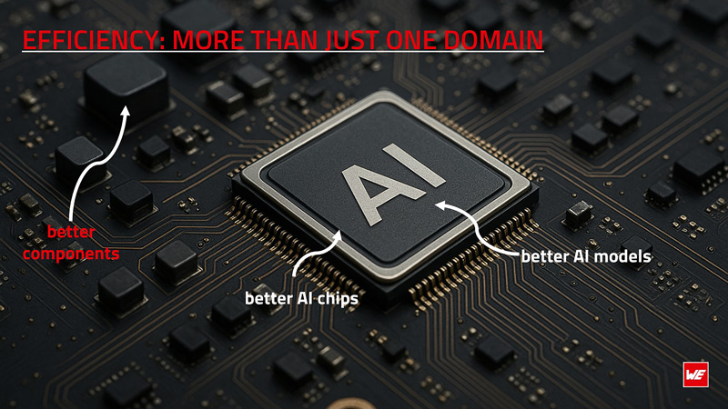
The efficiency gains that decide whether AI scales sustainably are hidden in the inductors, capacitors and delivery architecture between the grid and the processor.
Figure 1: With AI data-centre power consumption scaling toward thousands of terawatt-hours, overall system efficiency is increasingly decided in the power delivery network between the grid and the processor
AI has become the single most important driver of data-centre electricity demand. According to the International Energy Agency's “Energy and AI” report, published in April 2025, data centres worldwide drew around 415 terawatt-hours in 2024, roughly 1.5 percent of global electricity demand. In the agency's base case that figure more than doubles to around 945 terawatt-hours by 2030, growing by around 15 percent a year, more than four times faster than the growth of electricity consumption in all other sectors combined.
The aggregate figures reflect cluster, rack and accelerator power levels that have risen sharply within a few product generations. xAI's Colossus site in Memphis went into operation in 2024 with 100,000 H100 GPUs and a connected load of about 150 megawatts, comparable to a mid-sized industrial plant. Training, however, is not where most of the energy goes. Once a model is in production, everyday queries dominate: current estimates put 80 to 90 percent of AI computing capacity on the inference side. The move toward agentic systems steepens the curve further. According to Gartner, an agent that plans, calls tools and iterates autonomously consumes five to thirty times the tokens of a single chatbot exchange.
For power electronics, this is not an abstract sustainability debate. It is a design brief. Every watt an AI accelerator consumes has to be converted, delivered and filtered, and every conversion step that falls short of perfect efficiency turns the difference into heat that then has to be removed. Losses therefore appear twice on the bill: once at the converter, once at the cooling plant.
The Overlooked Lever
Discussion of AI hardware fixates on the processor: the GPU, the NPU, the accelerator die. The components that feed and stabilise that die attract far less attention, even though they increasingly determine how much of the incoming energy reaches the transistors. In general-purpose computing, inductors and capacitors can be selected from a catalogue. In an AI server they cannot.
A fully enabled Blackwell B200 is rated at up to 1,200 watts at package level, against 700 watts for its Hopper predecessor. A single rack built from such accelerators can draw more than 100 kilowatts. Rapid changes in switching activity produce steep di/dt load transients, and containing the resulting voltage excursions requires a hierarchical decoupling network: bulk storage, mid-frequency capacitance and low-ESL ceramics placed directly beneath the package. A GB200 board carries roughly 6,500 MLCCs, and the projection for the Rubin generation is about 12,000; AI servers carry ten to fifteen times the MLCC count of a general-purpose server. Passive components therefore shape both the electrical behaviour and the bill of materials of an AI system. They pose a first-order engineering problem spanning material science, packaging and converter topology.
Three developments are reshaping this layer in parallel;
Silicon Inductors
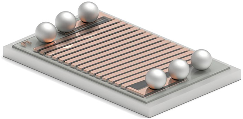
The first is the migration of magnetic components into the semiconductor process itself. Conventional wound or molded inductors occupy board area and sit centimetres from the load, a distance that becomes costly once currents reach hundreds of amperes, especially as switching frequencies increase. Thin-film inductors fabricated with semiconductor-like processes, often described as magnetics on silicon, allow the magnetic element to be integrated into the package, the substrate or directly onto the processor die rather than mounted beside it. Würth Elektronik has brought such solutions to market with partners. In joint development work with GlobalFoundries, these inductors are fabricated on 300-millimetre wafers in a standard CMOS lithography process, with electroplated copper windings, a sputtered and laminated core about six micrometres thick, a substrate thinned to 120 micrometres and a magnetic structure of roughly 80 micrometres, yielding a total chip height of roughly 200 micrometres. A 20-megahertz buck converter prototype built around a 187-nanohenry device reached a peak efficiency of 79 percent.
The advantage is the short distance to the load. Placing the inductor a fraction of a millimetre from the die shrinks the current loop and cuts parasitic resistance and inductance in the delivery path. It also supports the high switching frequencies that GaN devices enable in the low-voltage classes typical of point-of-load conversion. Higher switching frequency permits smaller inductance and capacitance values, though the required values are set jointly by control-loop bandwidth, ripple budget, ESR, ESL and the transient profile rather than by frequency alone. In multi-phase converter topologies, where the high load current is distributed across several phases, coupled-inductor structures push current density higher still. For high-current, low-voltage rails close to the processor, integrated inductors are a viable option. Their suitability depends on the required current, converter topology, thermal coupling, the loss budget, from DC resistance and core losses to skin and proximity effects, and manufacturing strategy.
Click image to enlarge
Vertical Power Delivery
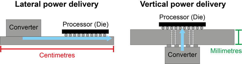
The second development concerns how power reaches the die. In a classic board layout, current travels laterally from converter to processor. Peak currents in today's designs reach up to 2,000 amperes, and the resistive drop in that horizontal path turns punishing: a lateral design supplying 800 amperes at 0.8 volts through a 70-microhm power-delivery network (PDN) dissipates about 45 watts in the delivery path alone.
Vertical power delivery reorganises the geometry. The final conversion stage sits underneath the processor and delivers power straight up into the package. The conduction path collapses from centimetres to millimetres, and losses fall precisely where currents are highest: a vertical 1,200-ampere design brings PDN resistance down to around 10 microhms and dissipates under 15 watts. How much of that loss is actually avoided depends on copper cross-section, layer stack-up, via resistance, package interconnects, current sharing and the exact placement of the final conversion stage. But the decisive move is architectural rather than at component level.
Click image to enlarge
Film Capacitors
The third development is unfolding in the dielectric. Data centres are moving from 48- to 54-volt distribution to 800-volt DC architectures. The driver is GPU power that a 48-volt bus can no longer carry efficiently. The change affects the rack feed and the intermediate bus; the final point-of-load stage still steps down to core voltages below one volt. Higher bus voltages raise the demands on insulation coordination, protection concepts and DC-link capacitors. Film capacitors are the workhorses of these DC links because they tolerate high ripple currents and, depending on construction and fault mode, exhibit self-healing behaviour, but their traditional weakness is energy density.
Efficiency Measured in Households
It is tempting to read these three developments as incremental gains. At the scale AI is reaching, they are not. Consider the arithmetic of a single percentage point. Saving one percent of the electricity that data centres are projected to consume in 2030 in the IEA base case amounts roughly 9.5 terawatt-hours – the annual electricity use of two to four million European households, depending on whether the household figure is taken at 4,700 or 2,400 kilowatt-hours a year. The figure assumes the gain is realised end to end across conversion and distribution, at unchanged utilisation. A parameter that a datasheet gives to one decimal place decides terawatt-hours at fleet scale.
In machine learning, a single point of accuracy is celebrated. The electrical efficiency of the system that runs the model deserves the same scrutiny: across tens of thousands of units in continuous operation, a point of efficiency adds up to gigawatt-hours and to operating cost that recurs every year.
Rethinking Power from Material to Algorithm
AI's energy trajectory cannot be corrected at any single layer. Better models help. Smarter distribution of workloads between cloud and edge helps, and so does a more efficient processor architecture. But energy lost in conversion and delivery cannot be recovered further up the stack. Efficiency has to be engineered at every level: from the magnetic material and the dielectric, through the inductor and the capacitor, into the delivery architecture, and only then up to the software.
For component manufacturers this marks a change of role. Supplying a catalogue part against a fixed specification is no longer enough when the specification itself is what is under negotiation: switching frequency, ripple budget, transient response, DC bias behaviour, losses across the operating range, thermal coupling, EMC performance, layout constraints and reliability under mission-profile conditions. The task becomes co-engineering: shaping the power path alongside the customer from the first architecture decision. In high-density systems, passive components and the delivery architecture determine efficiency, availability and cost of operation.
AI will not become less power-hungry on its own. Whether it scales in a way the grid and the climate can absorb depends less on the next headline model than on an unglamorous discipline: converting and delivering electricity as efficiently as physics allows. That work begins quietly in the passive components.