AIST researchers create a novel Tunnel FET architecture with potential to substantially improve device performance
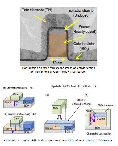
The tunnel field-effect transistor (tunnel FET) is a transistor that is based on electron tunneling and that, in principle, can switch on and off at lower voltages than the operation voltage of the metal oxide semiconductor field effect transistor (MOSFET). Its use therefore is expected to reduce the power consumption of electronic devices. However, the fact that the current through the tunnel FET is smaller than the current through the MOSFET has been an issue in practical application of the tunnel FET. The tunnel FET with the new architecture uses a new channel and electrode structure to allow a higher electric field to be applied at a specific gate voltage, and it has achieved an operating current 10 to 100 times that of conventional tunnel FETs. The developed tunnel FET is expected to help to reduce the power consumption of large-scale integrated circuits (LSIs). The social background The widespread use of electronic information devices such as mobile devices and high-performance personal computers and the increase in the amounts of information processed by these devices cause the increased energy consumption of the devices. There is a social need to reduce the power consumption of these devices. However, the reduction in power consumption of the MOSFETs used in today's electronic circuits is reaching the fundamental limit. To break through this limit, the tunnel FET, which operates on a principle different from that of the MOSFET, is attracting attention. Because, in principle, the tunnel FET can switch on and off at lower voltages than the operation voltage of the MOSFET, the power consumption of the electronic circuits using it is expected to be reduced. History of Research The Collaborative Research Team Green Nanoelectronics Center (GNC) was established in April 2010 to implement a project selected for FIRST, which is managed by the Japan Society for the Promotion of Science. The members of the team are researchers from five companies (Fujitsu Ltd., Toshiba Corporation, Hitachi Ltd., Renesas Electronics Corporation, and ULVAC, Inc.) and AIST researchers. Since 2011, GNC has been developing a tunnel FET and a compact model for operating this device, with the goal of reducing power consumption of LSIs to 1/10 to 1/100 of that of conventional ones. This research and development project was supported by the FIRST project "Development of Core Technology for Green Nanoelecronics" (Lead researcher: Naoki Yokoyama). Details of Research When a gate voltage is applied to the gate electrode of a tunnel FET, the width of the barrier between the source and the channel decreases owing to the effect of the electric field. As a result, the electrons pass through the barrier because of the tunneling effect and current flows through the transistor. Based on this principle, the tunnel FET can switch the current on and off at a lower voltage than that of conventional MOSFETs. The very fast switching of the tunnel FET enables the design of low-power electronic circuits that can operate at lower voltages However, because of the use of the tunneling effect, the tunnel FET has the disadvantage that the current passing through it is smaller than that through the MOSFET. To obtain a higher current efficiently, it is important to apply a stronger electric field to the tunnel junction. A high gate voltage is required to apply a strong electric field, while the tunnel FET needs to operate at a lower gate voltage to reduce power consumption. Therefore, the researchers used a new channel and electrode structure that can achieve a stronger electric field at the same gate voltage. In the tunnel FET architecture, after a very thin non-doped channel layer is epitaxially grown on a source with a high concentration of impurities, a three dimensional transistor is formed by placing a gate electrode around the double-layered channel. Conventional tunnel FETs are designed to switch the current on and off by using the effect of only the electric field perpendicular (a) or parallel (b) to the electric field from the gate electrode. In the new architecture, the vertical and horizontal electric fields are superimposed at the interface on the three dimensionally structured channel side-wall between the high-concentration source and the non-doped channel layer, making it possible to apply a stronger electric field than in conventional architectures. The researchers named the tunnel FET with this new architecture a synthetic electric field tunnel FET (SE-TFET). In the relationships between the gate voltage and the drain current obtained in a conventional tunnel FET and in the developed SE-TFET, the drain current was 10 to 100 times higher in the SE-TFET than in the conventional FET. Because an electric field even stronger than this can be applied to the tunnel junction by reducing the thickness of the epitaxially grown layer and the channel width, the performance of the SE-TFET can be improved by device scaling. In addition, although silicon (Si) was used in the developed SE-TFET, the new architecture can be effectively applied to tunnel FETs that use germanium or compound semiconductors including indium gallium arsenide; the performance of devices made of such materials exceeds the performance of those made from Si. Performance can be further improved in future by device scaling and advances in materials. The researchers will continue to optimize the process aiming at the low-voltage operation of complementary metal-oxide-semiconductor (CMOS) circuits. Also, they intend to develop an SE-TFET with much higher performance than that of conventional tunnel FETs and to reduce the operating voltage through further miniaturization. By combining the use of experiments, simulations, and circuit compact models, they will investigate the reduction effect on the power supply voltage when it is applied to CMOS circuits. AIST


