Application of Power MOSFET in Battery Management Charge-Discharge System
Power MOSFETs are connected in series between the inside of the lithium-ion battery pack and the output load
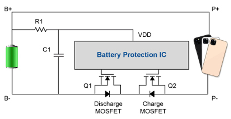
Figure 1. Battery protection board circuit diagram
Power MOSFETs are required to be connected in series between the inside of the lithium-ion battery pack and the output load. At the same time, the dedicated IC is used to control the on and off of MOSFET for managing the charge and discharge of the battery, as shown in Figure 1. In consumer electronic systems, such as cell phones, laptops, etc., the circuit system with control IC, power MOSFET, and other electronic components is called Protection Circuit Module PCM.
In the PCM, one power MOSFET is used for charging and another for discharging. The Power MOSFETs are connected in series, back-to-back, in two configurations. One configuration is when two power MOSFETs drains are connected. In the second configuration, the two power MOSFETs sources are connected. In addition, there are two ways to place the power MOSFET in series with the battery. One way is to place it on the negative end of the battery, called the "ground end" or low side; the other one is to place it at the positive end of the battery called the high side. The two different power MOSFET back-to-back connection modes and their different placement have their advantages and disadvantages, corresponding to different system requirements.
The PCM requires a low on-resistance MOSFET, so N-channel power MOSFETs are usually used. Some applications use P-channel MOSFETs on the positive end due to simple and flexible driving. However, P-channel MOSFETs on-resistance is relatively higher than N-channel MOSFETs and the selection is also limited.
Power MOSFET Connected Back-to-Back
The Working Principle
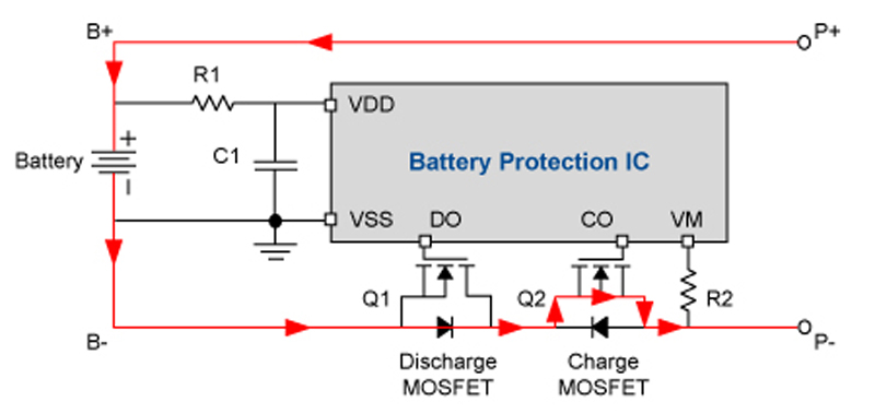
Two N-channel power MOSFETs to manage charge and discharge are placed at the ground end, and the drains are connected back to back, which is one of the common schemes of PCM, as shown in Figure 2. Where, Q1 is the power MOSFET for battery discharge, Q2 is the power MOSFET for battery charge, B+ is the positive end of the battery, B- is the negative end of the battery, P+ is the positive end of the battery pack, P- is the negative end of the battery pack, VSS is the ground of the battery protection management IC, the negative end of the battery, VSS and the source of Q1 is connected. Before PCM board work, Q1, and Q2 are both off.
(1) Charging
When charging, the control IC gate provides the driving signal CO to the charging power MOSFET(Q2), and the driving signal path of the Q2 gate is: The positive end of the external charging circuit→ P+→B+→R1→VDD→CO→Q2 Source →P-→The negative end of the external charging circuit. When Q2 is on, the charging current path is: P+→B+→B-→Q1 internal parasitic diode→Q2 channel→P-. The battery can then be charged, as shown in Figure 2.
Click image to enlarge
Figure 2. Charging loop when Q2 is on
To reduce the loss of Q1, when Q2 is turned on, the DO pin of the control IC is pulled high to make the discharge power MOSFET Q1 turn on. Due to the low RDSON of Q1, its conduction loss is far lower than that of the parasitic diode and the efficiency of charging could be improved. When Q2 and Q1 are in the on-state at the same time, the charging current path is: P+→B+→B-→Q1 channel→Q2 channel→P-.
(2) Discharging
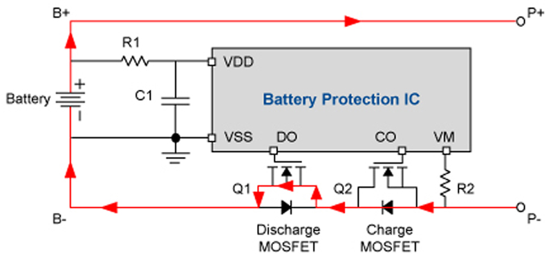
When discharging, the control IC provides the gate drive signal DO to the discharging power MOSFET(Q1), and the gate drive signal path of Q1 is: VDD→DO(Output of driver)→Q1 gate→Q1 Source→B- →VSS.
When Q1 is on, the current path of discharge is: P-→Q2 internal parasitic diode→Q1 channel→B-→B+→P+. The battery can then be discharged, as shown in Figure 3.
Click image to enlarge
Figure 3. Discharge loop when Q1 is on
To reduce the loss of Q2, when Q1 turns on, the control IC provides the gate drive signal CO to the charging power MOSFET Q2 so that Q2 is turned on. Q1 and Q2 are in the on-state at the same time.
Performance Requirements of Power MOSFET
Ion battery capacity from the early 600mAh, 1000mAh, to now has reached 6000mAh, 10000mAh. To achieve a faster-charging speed and shorter charging time, the fast charging technology of increasing current and charging with a large current is usually adopted. Then, the large current charging puts forward higher technical requirements for the power MOSFET in the battery pack. In addition, there are some specific technical requirements for large-capacity lithium-ion batteries in the production line and the using process.
High Power Density, Low Power Consumption, Good Heat Dissipation
The basic requirement of a large-capacity lithium-ion battery pack design is to improve the capacity of the battery as much as possible. Therefore, power MOSFET is required to have a smaller size and have the minimum on-resistance RDS(ON) under a certain size limitation, such as 1.2mm*1.2mm. To achieve lower RDS(ON) in smaller chip sizes, the design is mainly optimized from wafer technology and packaging technique. It is necessary to improve the MOSFET cell density.
In PCM, the package wire resistance is completely removed by using a new chip-level CSP packaging technology.
Short Circuit Capability
The large-capacity lithium-ion battery in the application, especially in extreme conditions, such as the output load short, there is a very large current through the battery. When IC detected output over-current, it will delay for a period of time to make protection action. During the delay time, the operating current of MOSFET is very large, which requires MOSFET to be robust for large current stress. As a result, all lithium-ion batteries are required to do a short circuit test.
In theory, the larger the chip size, the stronger the robustness for short circuit current is. However, with the trend of smaller form factors, there will be a limit on the capability. Thus, the application circuit design needs to keep in mind the requirements needed to ensure a robust design to resist the impact of a large short circuit current.
Avalanche Robustness
The MOSFET Avalanche capability is important when the output end of the battery pack is a short circuit and the switch is off. The selection of the power MOSFET should include a sufficient avalanche capability determined by the application conditions.
Key Points of PCB And Thermal Design
The temperature of MOSFET usually does not exceed 65 Celsius degrees in a normal environment temperature. The PCM control board is generally assembled with the battery and the PCB size is a constraint and typically has a high thermal resistance. Thus, special considerations may be needed in the thermal design of the system. The current path is symmetrical between the top to the bottom of the board to maintain the current balance. Maximizing the copper area of the power path and adding some vias for dissipation on the copper pads near the MOSFET are good design tips to improve the heat dissipation capacity and reduce the temperature rise of the MOSFET.

Click image to enlarge
Figure 4. Heat sink: aperture 12 mil, spacing 25 mil
All of these factors pose strict technical design challenges for the charge and discharge management of power MOSFET in the large-capacity lithium-ion battery pack. AOS provides a wide range of high-power density MOSFET products for the battery pack applications. AOS’s latest AOCA33102 and AOCR36330are suitable for mobile phone quick charging applications with ultra-lowRDS(ON) and new chip-level CSP packaging, which help to reduce the temperature rise of the power MOSFET and improve its reliability.