Are you SiC of Silicon? – Part 6
Using Silicon Carbide (SiC) FETs in Data Center power supplies and telecom rectifiers
With the deployment of 5G Networks, we can expect a massive build out worldwide, requiring many high-quality telecom rectifiers to provide the needed power. To meet the need for improved efficiency, lower operating and lower BOM costs, there is renewed interest in WBG (wide bandgap) solutions. The same can be said for the efforts to push server power supplies to ever increasing levels of efficiency with minimal heat loss. Hyperscale data centers that power the digital economy, big data, IoT and artificial intelligence now operate with >30KW server racks, and highly sophisticated cooling management systems.
5G networks with larger antenna arrays (up to 64 transmit/64 receive), facilitating 100-1000X higher data rates, and serving the trillions of devices forming the Internet of Things, would appear to need a great deal more power. Many technological improvements have been made to cut the power required for each base station, but it is likely that a far greater number of base stations are necessary. To serve the sophisticated methods of power management, power supplies for these base stations must meet ever more stringent efficiency requirements from standby to full load conditions.
New offerings of SiC FETs make it possible to hit previously unachievable efficiency targets, and we examine the main topologies and device capabilities in this article. We discuss what we might see in this space where Si Superjunction, SiC FETs and GaN FETs all compete.
Some Basics
What these power supplies all have in common is a power-factor-correction PFC section, that rectifies the AC to DC at near unity power factor with an output voltage of 400V, followed by a DC-DC converter which converts this 400V to 48V or 12V for use within the system. Further point-of-load converters are then used to power the CPUs and Memory banks.
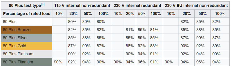
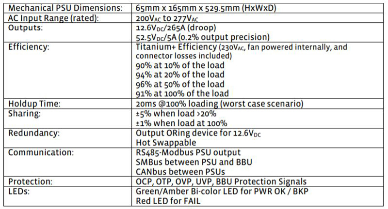
If one examines the usage profile of data center server power supplies, it becomes clear that a large portion of their operating life is spent at light to medium load. Therefore, the PFC and DC-DC sections must perform at high efficiency at all load conditions, while meeting the thermal constraints of peak load operation. This is captured by the well known 80 Plus standard used for computing power supplies, shown in Figure 1. Servers must meet the Titanium standard, which maintains high efficiency even at 10% load. Figure 2 shows a typical specification taken from the Open Compute Project, which features a Titanium+ requirement for a 3.3KW class power supply.
Click image to enlarge
Figure 1: 80 Plus standards showing efficiency targets for computing power supplies
Click image to enlarge
Figure 2: A 3.3KW server power supply specification taken from the Open Compute Project
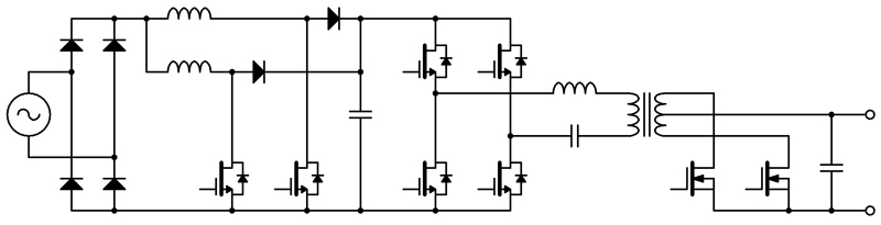
Figure 3 shows a typical power supply architecture with its input bridge rectifier, a simple dual interleaved boost converter (PFC) with a 650V FET and SiC JBS (Junction-Barrier-Schottky) diode as well as a full-bridge LLC stage for the DC-DC converter. The input EMI filter is not shown. Typical switching frequencies of 65-150kHz are used for the PFC stage. Here the need for power density is traded off against higher efficiency at lower frequencies, since the inductor can be made much smaller switching at 150kHz instead of 30kHz. This leads to the use of silicon superjunction MOSFETs with SiC JBS diodes to maintain high efficiency while hard switching at 65-150kHz. Highly advanced superjunction MOSFETs can switch fast, while the SiC Schottky diode helps minimize the turn-on losses in the MOSFET.
Click image to enlarge
Figure 3: A commonly used power supply configuration. After the input bridge rectifier, there is an interleaved PFC stage, and a full bridge LLC stage
In the LLC part of the circuit, 650V MOSFETs are also commonly used. The circuit maintains ZVS (zero voltage switched) operation and has reduced turn-off currents, so losses are much lower, allowing higher frequency operation at 100-500kHz, which in turn allows the transformer to be made smaller. On the secondary side, very low on-resistance 80-150V silicon MOSFETs are used to rectify the high frequency secondary AC voltage to provide the regulated output DC voltage. The 650V FETs used are selected so that in the event ZVS is lost under some operating conditions, the body diode recovery is not destructive.
Semiconductor Devices
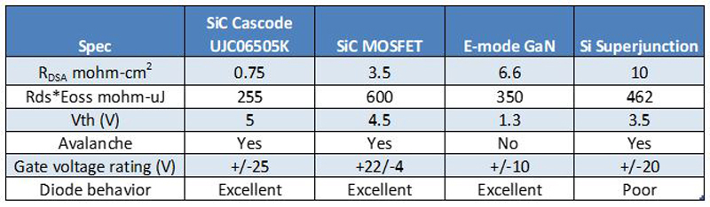
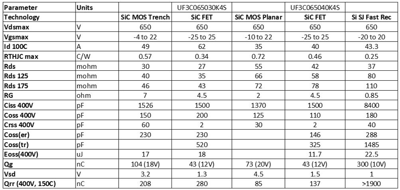
Focusing on the transistors, on the high voltage side of the PFC and DC-DC units, 650V class devices are commonly used. Table 1 provides an overview of the current state of the art for silicon, GaN and SiC devices and their relevant characteristics. In terms of RdsA, which translates to chip size, the SiC FET (SiC JFET RdsA) is by far the best option. All the wide bandgap devices offer excellent body diode recovery improvement over the silicon superjunction alternative. However, only the SiC and silicon devices are capable of handling avalanche energy. The enhancement mode GaN devices also have a low Vth, which coupled with their speed and narrow gate voltage range, makes them harder to drive.
Click image to enlarge
Table 1: Basic technology comparison of 650V transistor options
Table 2 shows a comparison of some industry equivalent products in the commonly used TO247 package. The silicon superjunction (Si SJ) device and the UnitedSiC can be driven by 0 to 10V drive. The SiC MOS options require different voltages (for e.g. -4V to 18V). The SiC devices all offer lower input capacitance (gate charge) and much reduced diode recovery charge Qrr. The body diode conduction losses of the sSilicon superjunction and SiC FET are lower than those of SiC MOSFETs.
Click image to enlarge
Table 2: Parameter comparison of similar transistors in a TO247 package type
Table 3 shows a comparison of similar devices in DFN8x8 footprint. The silicon SJ, SiC FET and GaN device can all be driven by standard silicon gate drives. UnitedSiC FETs offer very low on-resistances. Comparing devices with different 150 deg C RDS(ON) is best done using the figures of merit in the bottom three rows. The WBG solutions offer better figures of merit, especially for Rds*Coss(tr) and Rds*Qrr.

Click image to enlarge
Table 3: Parameter comparison of Si drive compatible transistors in a DFN8x8 package type
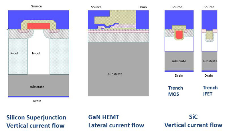
Figure 4 shows the cross-sectional architecture of commonly used configurations of SiC, GaN and silicon superjunction FETs. GaN HEMTs are lateral devices, while the other device types are vertical current flow devices. Vertical current flow allows higher voltage devices to be implemented more compactly, since the source and drain terminals are on opposite sides of the wafer, and not both on the top surface. In the GaN HEMT, conduction is confined to the 2DEG channel, while the SiC devices use a short surface channel, but mostly the bulk for carrying current. The SiC JFET has a bulk channel, which along with its vertical nature, results in the lowest resistance per unit area (RdsA) and allows the lowest chip size. It is then cascoded with a low voltage Si MOSFET (which adds 10% to the resistance), to form the SiC FET.
Click image to enlarge
Figure 4: Architecture of semiconductor devices that compete in the 650V space used for data center and telecom power supplies
As devices improve, the ultimate switching speed limit is set by the load current charging the device output capacitance Coss. A low value of Coss(tr) for a given on-resistance gives the fastest slew rate, as well as the shortest delay time to reach 400V. It is clear from Table 3 that the SiC FET is excellent in this regard, and a good choice for high frequency power conversion.
In terms of Qrr, the WBG options all offer much improved performance compared to silicon superjunction devices. Therefore, these devices are selected whenever the circuit uses hard-switched turn-on as in a CCM (continuous current mode) totem pole PFC. If these circuits use body diode conduction in the freewheeling state, the on-state drop of the body diode leads to conduction losses. Therefore, synchronous conduction is generally used, turning on the FET channel to reduce these losses. There is usually a delay between detecting the current reversal and turning on the FET channel, and this time becomes a significant fraction of the switching period at high frequencies. For example, a 100ns dead time where the diode conducts matter little if the switching frequency is 100kHz (10us period). But is becomes 10% during a 1MHz (1000ns period) switching cycle. Therefore, low body diode conduction drop VSD together with low Qrr is a useful characteristic and SiC FETs provide both.
Moreover, the most efficient circuit options avoid hard switched turn-on, because while turn-off losses can be made negligible with WBG devices, this is not the case for turn-on losses. With the low gate charge of available FETs, and low on-resistance and turn-off losses, frequencies in soft-switched circuits can be pushed up by 5-10X.
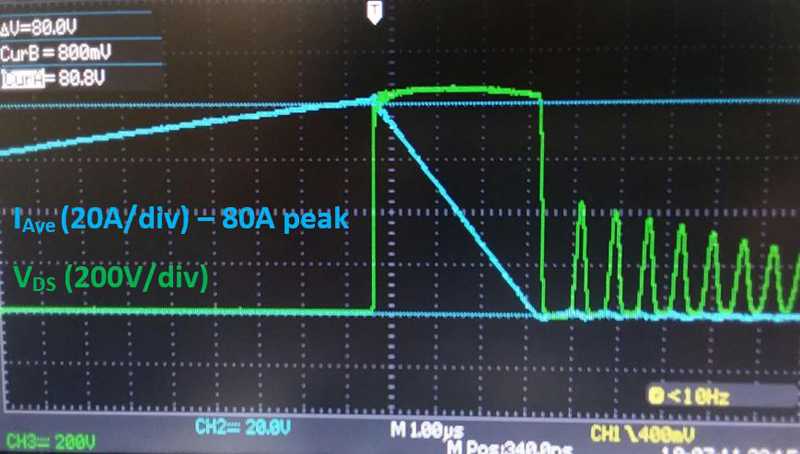
In terms of device robustness, all SiC options offer excellent avalanche capability, which enhances the system reliability of the converter. Despite their smaller chip sizes, they can often exceed the capability of superjunction FETs especially at high current levels. GaN devices cannot handle avalanche and are therefore designed with high breakdown voltages to avoid this operating zone. Figure 5 shows a scope capture of a 40mohm, 650V SiC FET from UnitedSiC handling 80A peak avalanche current (blue), far in excess of any practical need. Breakdown voltage is seen to be over 800V (green).
Click image to enlarge
Figure 5: Unclamped inductive test waveform for UF3C065040K4S, a 40m, 650V SiC FET device. Despite a small SiC JFET size, the device handles a over 80A avalanche current without failure
Gate Drive Considerations
A key simplification using SiC FETs is that in the low voltage MOSFET has a 5V threshold VTH, and a VGS(MAX) rating of +/-25V. It can be driven like a silicon superjunction MOSFET from 0 to 10V (or 12V). Figure 6 is a comparison of the recommended gate drive voltage for various technologies and the corresponding gate absolute maximum ratings. SiC MOSFETs usually employ negative and positive gate drive and need a 20 to 25V total swing in gate voltage. The gate voltages are often quite close to the absolute maximum ratings, which requires careful attention to gate spikes. The large gate swing can add up to considerable gate charge loss at higher frequencies. Furthermore, to manage the VTH hysteresis issues, the manufacturers’ recommendations must be carefully followed for gate drive voltage levels. SiC FETs are flexible in this regard, do not require such careful control of gate voltage levels, but can also be driven at gate voltages compatible with SiC MOSFETs.

Click image to enlarge
Figure 6: Chart comparing the recommended gate drive and gate voltage maximum ratings for various Silicon and SiC device types. The SiC FET is uniquely versatile
GaN enhancement mode devices generally have a low Vth, and are driven in a narrow gate voltage range, which is often quite close to the absolute maximum VGS limits. This requires specialized drivers and careful layout to avoid damage to the switches. The cascode option can circumvent some of these difficulties. The lower gate voltage swing of enhancement mode devices is beneficial in reducing gate losses at higher frequencies.
In all instances, as the devices are used at higher speeds, holding the devices off at high dV/dt becomes increasingly challenging. As does the management of gate voltage spikes from the power loop and gate drive loop inductances. Introduction of packages with source kelvin pins has helped, but we look at other options in a later section of this article.
Circuit Topologies – PFC stage
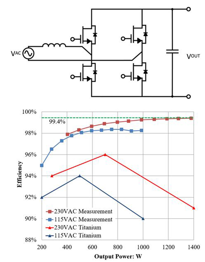
Figure 7 shows a Totem-Pole PFC (TPPFC) circuit, and the measured efficiency at 100kHz on a UnitedSiC demonstration board at 1.5KW using the UJC06505K SiC FET. This circuit eliminates all the diode conduction losses, both from the input diode bridge and the SiC PFC diode. In this case, the converter operates in CCM mode, and the devices are hard switched.
Click image to enlarge
Figure 7: A basic Totem-Pole PFC circuit, and efficiency data compared to the Titanium standard, measured on the UnitedSiC demonstration board using UJC06505K (SiC FET)
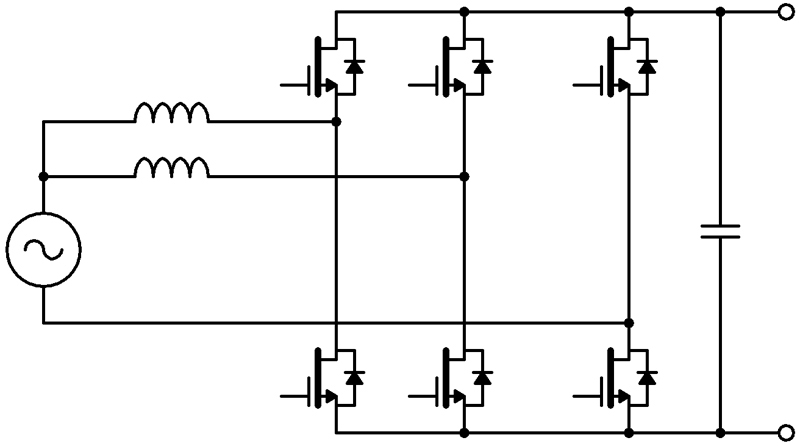
Figure 8 shows an interleaved TPPFC which can be designed with a coupled inductor. This circuit can be used in continuous current mode, or it can be operated at a much higher frequency in critical conduction mode since that eliminates turn-on losses. A very high-power density can be achieved using SiC FETs without sacrificing efficiency, although the complexity in control and magnetics design is greater when ripple currents are high and current zero crossings have to be detected.
Click image to enlarge
Figure 8: Interleave Totem-Pole PFC, which employs two fast switching and one line-frequency switching half-bridge. A coupled inductor approach allows the use of critical conduction mode operation, allowing a significant increase in frequency
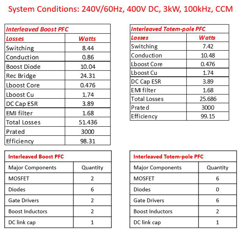
Table 4 shows a comparison of the loss breakdown using the interleaved PFC topology shown in figure 1 and the interleaved Totem-Pole PFC of figure 8. In both cases, we assume a 3KW class converter, operating each switch at 100kHz. The interleaving means the inductors see a ripple frequency of 200kHz. The Totem Pole PFC has much reduced losses of 25.7W vs 51.4A, making it possible to achieve Titanium net efficiency targets. This is driven by eliminating the 24.3W loss from the bridge rectifier. The Totem-Pole PFC used in this example does require four more FETs and gate drives.
Click image to enlarge
Table 4: Loss and complexity comparison of a Interleaved PFC and Totem Pole PFC circuit using UJC06505K to achieve 3KW at 100kHz in CCM mode
An alternate method that does not require detection of current crossings uses additional auxiliary switches to achieve zero voltage transitions at turn-on. Similar or better results can be obtained using resonant techniques such as the auxiliary resonant commutated pole (ARCP) that eliminate both turn-on and turn-off losses. However, the cost-performance benefits of the more advanced techniques seem to be favorable only at power levels well above 5KW.
Circuit Topologies – DC-DC stage
Since the output voltage is fixed, the full-bridge LLC converter of figure 1 offers excellent power density and efficiency, and is presently the industry workhorse at higher power levels. As power levels get lower, a half-bridge LLC implementation may be used. Frequencies in the 100-500kHz range are commonly used, and the key effort in loss reduction shifts to the transformer secondary and low voltage secondary MOSFETs, given the high current levels at the 12V output.
For the high voltage FETs, the VDS transition from its off-state to diode conduction requires charging the output capacitance, and in order to do it quickly, a low COSS(TR) is necessary. However, users must then minimize the dead time before gating on the FET for synchronous conduction to reduce the loss from body diode conduction. A low resistance in the on-state minimizes conduction losses, and the low EOFF of most superjunction and WBG switches helps keep switching losses at a minimum.
If under light load conditions, ZVS is lost, diode hard recovery can occur. With WBG switches such as the SiC FET, this poses no risk, but can damage silicon superjunction MOSFETs. To minimize this possibility, fast recovery versions of superjunction FETs are often used, but no such precaution is needed with SiC FETs.
Outlook for the Near Future
While improvements in silicon superjunction FETs continues, the levels of improvements possible for SiC and GaN devices in the next few years far outstrips what can be achieved with silicon. In addition to improvements in RdsA (improvements of 30-50% every 2-3 years), many improvements in package technology are to be expected. The main challenges being addressed are low inductance, and more efficient heat removal in small surface mount options.
One likely path is the migration to half-bridge elements designed either for direct surface mount use, or as an embedded element in the PCB. This simplifies PCB layout and allows the implementation of lower inductance power and gate loops.
Another emerging path as the integration of the driver with the power device, either as a single driver plus switch, or as a half-bridge element. Since most SiC and GaN devices need unique driving voltage levels and circuits, this complexity can be absorbed into the co-packaged or integrated product, making this easier for users. In addition, each device can then be better utilized to its full potential. This will no doubt lead to greater savings in system cost and power losses, and drive WBG adoption.
Along these lines, the SIP half-bridge with an integrated half-bridge gate drive using 35m, 1200V SiC FETs was described in previous articles in this series. Surface mount options are emerging from various suppliers, and the trend is likely to accelerate.
The cost of 650V wide bandgap switches is now dropping rapidly. UnitedSiC 650V FETs are expected to approach price parity with silicon within the next two years. Along with the ease of use, this is expected to rapidly accelerate the deployment of WBG devices in server and telecom power supply applications.
UnitedSiC