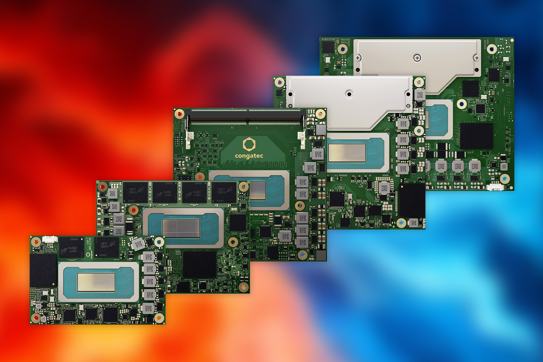
For years, AT&S has worked at the forefront of process and technology development to meet the challenges of continued miniaturization and the demand for better energy efficiency. In this context, the company is involved in various research and development programmes. One current example is the Horizon 2020 EU Research and Innovation programme, in which 11 key European actors are collaborating on the GaNonCMOS project. AT&S is also participating in the Panel-Level Packaging Consortium managed by Fraunhofer IZM.
Optimized energy efficiency with GaN
Over the next four years, the GaNonCMOS project consortium – including AT&S – intends to develop cost‑effective and reliable GaN-based processes, components, modules and integration approaches. In particular, the project aims to exploit the energy-efficiency advantages of GaN (gallium nitride), targeting the production of several demonstrators with GaN power switches and CMOS drivers, as well as new magnetic core materials that will enable switching frequencies up to 200 MHz. Together with optimized embedded PCB technology, the developments should lead to new integrated power components for low-cost, high-reliability systems. Working alongside AT&S on this project are the University of Leuven, Epigan, Fraunhofer, IBM Research, IHP, Tyndall National Institute, PNO Innovation, Recom, NXP Semiconductors and X-FAB Semiconductor.
Advancing miniaturisation with panel-level packaging
The Panel-Level Packaging Consortium has also now been formed. It comprises internationally leading partners such as Intel, ASM Pacific, Hitachi Chemical, AT&S, Evatec, Nanium, Süss MicroTec, Unimicron, Brewer Science, Fujifilm Electronic Materials U.S.A., ShinEtsu, Mitsui Chemicals Tohcello and Semsysco. Together with Fraunhofer IZM as the development hub, the plan is to implement fan-out panel-level packaging (FOPLP), one of the newest packaging trends in microelectronics. FOPLP has a very high miniaturisation potential in both package volume and package density.
During the consortium’s two-year term, known technological elements in wafer-level packaging will be transferred to a large panel format. The technological basis for FOPLP is a reconfigured, moulded panel with embedded components and a thin-film redistribution layer, which together yield an SMD-compatible package. The main advantages of FOPLP are a very thin, substrateless package, low thermal resistance, and good RF characteristics. In addition, passive components such as capacitors, resistors, inductors and antenna structures can be integrated into the redistribution layer. This makes the technology suitable for creating multi-chip packages and System-in-Packages (SiPs).
Based on a panel size of 18" x 24" (a PCB manufacturing standard) or even larger sizes, lower packaging costs can be achieved thanks to higher productivity.