Augmented Reality and the Internet of Things
Circuit protection technologies and board layout strategies that promote safety, reliability, and connectivity
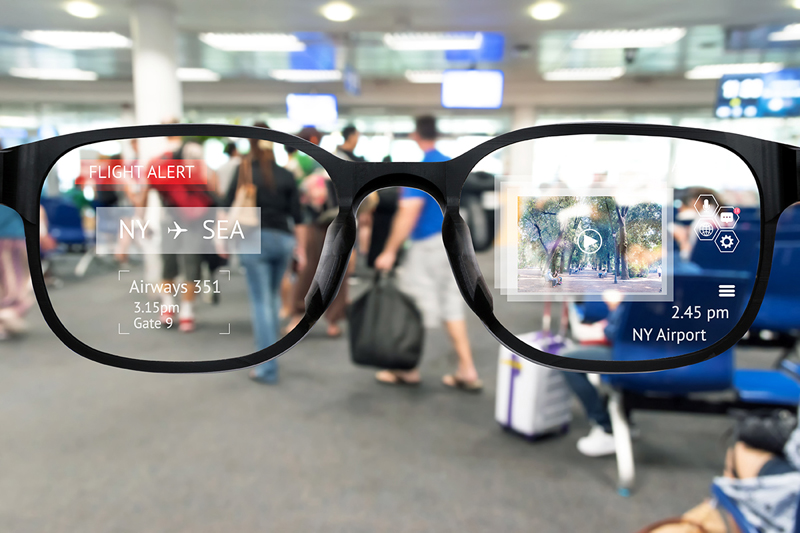
Figure 1: Augmented Reality (AR) glasses displaying airline flight information
For those of us who wear glasses for vision correction, we are used to seeing the world through lenses. However, new technologies will allow a virtual world to be laid on top of the real world that we normally see. In other words, the lenses will become displays that allow us to see the “real” world that is augmented with overlaid information and images, creating an Augmented Reality (AR). An example would be the integration of navigation into the AR glasses to allow a user to walk through town with turn-by-turn instructions (visual or verbal) to help them easily get to their destination. Other examples include facial recognition, fitness tracking, first-person photos and videos, as well as health-sensing and travel applications (Figure 1).
With the continued decrease in the size of microprocessors, and the inverse increase in computing power, it is now possible for the lenses to become displays that enhance the world that we see. And the forecast is bright indeed. There are forecasts that predict growth of about 150% between now and 2024. In order for there to be broad market acceptance, the products will have to deliver on the promise of the technology to enhance our perception of the world around us, and do so with quality and reliability throughout their functional lifetime.
The integration of these AR glasses into our lives as well as the broader IoT world demands advanced technology to protect the sensitive electronic components and circuits needed to maintain functionality and IoT connections. Since the glasses will be worn on our faces and next to the skin, they are constantly bombarded by static electricity generated by close interaction with the user. Without proper protection, the device’s sensor circuits, battery-charging interfaces, buttons or data I/Os could be damaged by electrostatic discharge (ESD).
This article will discuss advanced circuit protection technologies and board layout strategies that safeguard wearable devices and their users. Applying these recommendations early in the design process will help today’s circuit designers improve the performance, safety and reliability of their wearable technology designs and help build a more reliable IoT ecosystem.
Robust ESD Protection in a Small Form Factor
Providing adequate circuit protection for wearable devices has its own challenges caused by the need to continue shrinking the processors, memory, etc. that allow the AR glasses to have some much computing power. In the past, large diode structures and large package sizes (e.g., 0603 and 0402) were needed to achieve excellent ESD performance and low clamping voltages. However, with continued improvements in wafer fabrication processes and back-end assemblies, it is now possible to have very robust ESD protection in a small form factor. For example, a general purpose 01005 transient voltage suppression (TVS) diode from Littelfuse can withstand 30kV contact discharge (IEC 61000-4-2). It packs that robust ESD performance into a package with dimensions of only 0.4mm x 0.2mm! (See Figure 2.)
Click image to enlarge
Figure 2: As the sophisticated chipsets used in wearable devices get smaller and faster, the form factor and performance of the circuit protection devices must do the same
Why is robust ESD protection so important? While the test level used in the Human Body Model (HBM) specification for modern integrated circuits can reach 2,000V, most application designers ensure that their system meets at least Level 4 of the IEC 61000-4-2 test standard (8kV contact, 15kV air discharge). In many examples of portable devices and wearables, the contact discharge level has been raised to 15kV or 20kV, with some companies setting it as high as 30kV. This “mismatch” between what the processors can survive, and what they’ll experience in the field, needs to be addressed with robust ESD suppression technologies like those offered by Littelfuse, to ensure long-term operation and reliability.
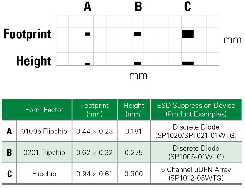
Selecting and applying modern ESD technologies can result in significant board area savings. For example, the most common discrete form factor for ESD Diodes is the SOD882 package, which has an outline of 1.0 mm x 0.6 mm. By moving to the 0201 form factor (0.6 mm x 0.3 mm), the designer can save approximately 70 percent in board area. Furthermore, moving to the 01005 outline yields a savings of over 85 percent compared to the SOD882 package. (See Figure 3 and table in Figure 1.)

Click image to enlarge
Figure 3: Products like the SP1020 from Littelfuse pack robust ESD protection in a very space efficient 01005 package; ideal for applications like AR Glasses where there is very little board space available
Despite the reduced form factor of wearables, today’s ESD diodes are able to deliver outstanding performance without any reduction in ESD performance. In fact, discrete semiconductors with a small form factor can have the same level of ESD robustness (30kV contact discharge) and low clamping performance (dynamic resistance < 1 Ω) as their larger counterparts (e.g., SOD323 and SOD123). However, the small size of the component may present manufacturing challenges. At 0.4 mm x 0.2 mm, the 01005 package will require well-designed board treatments such as solder pads and thick stencils to ensure that the component does not slide or “tombstone” during the reflow solder process.
Selection and Configuration Factors for TVS Diodes
As previously discussed, today’s ESD diodes offer a variety of performance benefits for Augmented Reality applications led by a small form factor. The following recommendations for the selection and configuration of ESD Diode technologies will help design engineers optimize their future circuit designs.
Choosing unidirectional or bidirectional diodes. ESD diodes are available in unidirectional or bidirectional configurations. Unidirectional diodes are typically used for DC circuits, including pushbuttons and keypads, as well as digital circuits. Bidirectional diodes are used in AC circuits, which may include any signal with a negative component greater than -0.7 V. These circuits include audio, analog video, legacy data ports and RF interfaces.
Whenever possible, design engineers should choose unidirectional diode configurations since the performance during negative-voltage ESD strikes is improved. During these strikes, the clamping voltage will be based on the forward bias of the diode, which is typically less than 1.0 V. A bidirectional diode configuration provides a clamping voltage during a negative strike that is based on the reverse breakdown voltage, which is higher than the forward bias of the unidirectional diode. Thus, the unidirectional configuration can dramatically reduce the stress on the system during negative transients.
Click image to enlarge
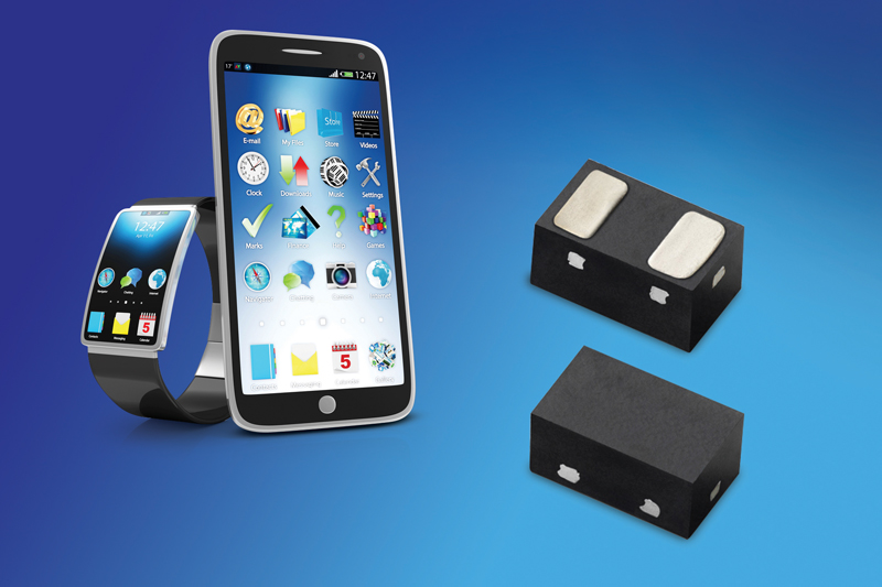
Figure 4: Low-capacitance bidirectional discrete TVS diode arrays, including the SP3022 Series, provide symmetrical ESD protection for high-speed data lines when AC signals are present. They are also designed for consumer electronics such as fitness bands, smart watches, smartphones, tablets and eReaders
Determine diode location. Most circuits do not require board-level ESD Diodes at each of the IC’s pins. Rather, the designer should determine which pins have exposure to the outside of the application where user-generated ESD events are likely to occur. If the communication/control line can be touched by the user, it could become a pathway for ESD to enter the integrated circuit. Typical circuits include USB, audio, button/switch, RF antennas and other data buses. Incrementally adding these discrete devices will take up board space, so it is important to reduce their size to fit 0201 or 01005 outlines. For some wearable applications, there are also space-saving multi-channel arrays available.
Consider routing of “ESD” trace. To protect the IC’s pins with an ESD Diode, there are several key considerations for trace routing—from I/O to ground. Unlike lightning transients, ESD does not unleash a large amount of current for a long duration of time. To effectively handle ESD, it is important to move the charge from the protected circuit to the ESD reference as quickly as possible. The length of the trace—from the I/O line to the ESD component and from the ESD component to ground—are the overriding factors, not the width of the trace to ground. The length of the trace should be kept as short as possible to limit parasitic inductance. This inductance would result in inductive overshoot, which is a brief voltage spike that can reach hundreds of volts if the stub trace is long enough. Recent package developments include µDFN outlines that fit directly over the data lanes to eliminate the need for stub traces entirely.
Understand HBM, Machine Model (MM) and Charged Device Model (CDM) definitions. HBM, MM and CDM are test models for characterizing the ESD robustness of the integrated circuits that run the portable device or wearable, including the processor, memory and ASIC. They are used by the semiconductor supplier to ensure the robustness of the circuits during manufacturing. The current trend is for suppliers to reduce the voltage test levels since it saves die space and because most suppliers adhere to excellent in-house ESD policies.
While strict ESD policies benefit the supplier, the application designer ends up with a chip that is very sensitive to application-level ESD, but must not be allowed to fail due to field-level or user-induced ESD. To succeed, the designer must select a board-level device that is robust enough to protect against intense electrical stresses yet offers low enough clamping to protect the highly sensitive integrated circuitry. When evaluating an ESD protection device, consider the following parameters:
1. Dynamic resistance: This value is a measurement of how well the diode will clamp and divert the ESD transient to ground. It helps determine how low the resistance of the diode will be after it switches on. The lower the dynamic resistance value, the better.
2. IEC 61000-4-2 rating: The ESD Diode supplier determines this value by increasing the ESD voltage until the diode fails, which characterizes the robustness of the diode. For this parameter, the higher the value, the better. A growing number of Littelfuse ESD Diodes can reach as high as 20kV and 30kV contact discharge, which far exceeds the highest level of the IEC 61000-4-2 (Level 4 = 8kV contact discharge).
Conclusion
The nascent market for Augmented Reality Glasses offers many interesting and useful opportunities for us as consumers. But, all those amazing capabilities will not be recognized if the glasses are not able to survive the daily bombardment of ESD transients generated by the wearer of the glasses. For this reason, it is more important than ever to consider ESD protection and proper board layout practices early in the design process to ensure that the application is reliable with a useful lifetime. Circuit protection devices like ESD Diodes are designed to be highly robust even with small form factors; preventing ESD damage to the AR headset and providing the user with years of reliable service. Designing in hardy protection for the sensitive integrated circuitry inside the wearable device is necessary to maintain the value proposition of the IoT ecosystem.
Littelfuse, Inc.