Power supplies are usually not designed with pen and paper anymore
For many years, engineers have used calculation tools to optimize a switch mode power supply design. In the early years, power supply engineers would program their own tools or use spreadsheets they generated themselves with the required formulas underlying a certain power supply topology. While this helped tremendously to speed up the design process, it was also a cumbersome task. In addition, the calculated results were often quite far from actual measurement results of real hardware.
The reason for this is that usually calculations were based on nominal values of ideal components and not on real components. Component values change over temperature, voltage, current, aging and manufacturing process. Considering these changes is possible, but requires a detailed database of real component values, not just nominal values, for selecting the right part. Only with such a database, a true optimization of a real design is possible. This kind of database should also include information about board area and cost for each component. With this, also board space necessities and the typical cost pressure designers have can be accounted for.
Design flow of a DC/DC converter
The design flow of a switching power supply is to first select a power supply topology and a suitable switching regulator or controller IC. Once the topology and switching regulator IC is selected, the circuit calculation can start which includes the selection of passive components. This process can be quite difficult, since the right optimization process needs to be applied. Usually a lot of power supply experience is required to achieve a good optimization.
In some cases, the selection process of the topology and switching regulator or controller IC cannot be completed without going through the optimization process very deeply. For example, sometimes it is not exactly clear if a SEPIC topology, a flyback or a boost topology followed by a buck topology has a better power efficiency at certain operating conditions.
This is why most of the effort of a design process is actually spent on the optimization. After the optimization, a circuit can be simulated and after possibly some minor tweaks were done, it can be built with real hardware. This is when the evaluation and testing period begins. In switch mode power supply design, there are many influences coming from parasitics, which come from board layout and non-idealities of passive components. Also, effects of near field coupling on the PCB by electric fields (capacitive coupling) as well as by magnetic fields (inductive coupling) will have an influence on the behavior of the switch mode power supply. These effects cannot easily be calculated and simulated. This is why even today, with very advanced design tools available, in most cases there is still no substitution for hardware evaluation of a switch mode power supply.
Circuit selection tool
Today most companies with a significant power supply regulator and controller IC portfolio offer some kind of circuit selector. The user would enter the minimum and maximum input voltage, the desired output voltage, output current and ambient temperature. Then a circuit selector will propose a switching power supply topology and a suitable regulator or controller IC.
For example, Analog Devices offers the ADIsimPower Selector tool for this task. Recently there has been renewed activity from a third party with a selection tool which is not only limited to one vendor of components, but to the whole industry. This can be quite useful to search different vendors at the same time. In the past such offerings would have limited success, since these databases where often not very accurate and could often not find the latest product offerings. It remains to be seen how future general market selection tools will perform. Figure 1 shows a screen shot of the Analog Devices Circuit selector tool. The top shows the typical specification window, and below is the list of proposed topologies and switching regulators and controllers.
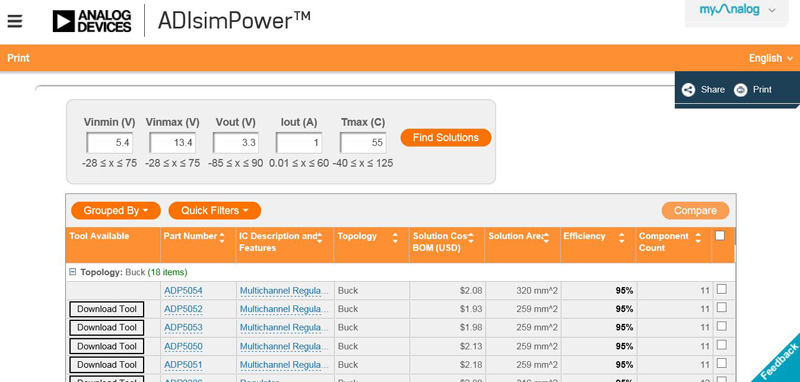
Click image to enlarge
Figure 1. Entering power supply requirements and below proposed solutions
Optimization tool
An optimization tool really helps with the most important design step in power supply development. This is where external components and possibly additional filter stages are selected. Coming up with ‘any design’ that will work is by far not as difficult as coming up with the optimized design in regards to specified requirements. This design step is very time consuming and difficult.
Optimization tools such as ADIsimPower Designer can help a great deal. They have an iteration process and calculate different designs in parallel and then ultimately report the best design according to pre-set optimization algorithms. When using such tools it is important to also learn about how a given tool is programmed to optimize.
The ADIsimPower Optimizer has thousands of real components included, which are used for the optimization, and then are suggested in the proposed optimized bill of materials (BOM). The components are included with very detailed information. Value changes over temperature are considered, but also less known data such as capacitance change with DC voltage across a ceramic capacitor or detailed core losses in an inductor are included.
Only if the components in the optimizer are modeled accurately, the optimized result will predict real behavior of a switch mode power supply closely. Since many tradeoffs in an optimization process are based on component cost, prices are included in the database as well. This fact makes it necessary for the optimization tool to get updated every few months. Component values typically do not change from month to month, component prices however might.
Compared to a circuit selector tool, a true circuit optimizer requires a greater knowledge of specification details. A general piece of information is if a design should be optimized for ‘lowest part count’, ‘lowest cost’, ‘highest power efficiency’ or ‘smallest solution size’. More detailed specifications include expected load transient steps and the amount output voltage variations are acceptable after such load transient responses.
Figure 2 shows a screenshot of the power supply design optimizer tool from Analog Devices. It displays calculated efficiency, losses, bode plot of the regulation loop and many other useful details about the proposed circuit. Each circuit optimizer comes with the possibility to order a blank, non-populated, evaluation board. Such a board comes with large enough pads to work with most possible selections of components. This board can greatly help in moving from the design step to the evaluation step which is always necessary in switch mode power supplies as mentioned before.
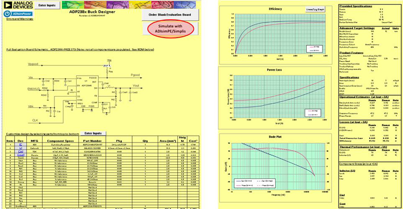
Click image to enlarge
Figure 2. Design and optimization tool
Simulation tool
Simulation tools are nice. They offer the capability to look at many different waveforms to get familiarized with the future circuit, and can also show interactions of the power supply with other circuitry if they all are simulated together. However, simulation tools cannot replace a thorough optimization process.
A power supply designer with little experience will have a hard time finding an optimized solution by only using a power management simulation tool. Very often designers start with a typical switch mode power supply circuit file in their simulator and then they try to modify the components to find a solution which fits the specification of the power supply under development. This usually requires a long iterative simulation process at which the final solution may not actually be the optimum. Don’t be tricked into thinking that a simulation will solve all design challenges for you.
After a thorough and successful design optimization with an optimization engine, simulations can offer good benefits. There are many different simulation tools on the market. Some are accessible online, others can be downloaded. Some cost money, while others can be used for free with a limitation on simulation nodes and the necessity to have a certain vendor’s components on the simulation schematic.
Spice-type simulators are widely used and popular, they are not so well suited for switch mode power supplies however. There are other simulators such as SIMetrix / SIMPLIS available which are more suitable for power management simulations. They can deal better with the switching transitions in a power supply and thus are much faster. Often by a factor of 10 to 50 compared to a typical Spice simulator. Also convergence errors are minimized.
For example, Analog Devices offers the ADIsimPE Simulator based on SIMetrix / SIMPLIS. It can be downloaded for free with a certain limitation of node quantities. The optimization tool described in the earlier chapter has a push button to start simulations with SIMetrix / SIMPLIS. It will export a file describing the final solution and this file is then used by the simulator directly.
Such a seamless transition into actual simulations requires very little simulation experience and knowledge. Figure 3 show the simulation schematic of the new ADP5070 in SIMetrix / SIMPLIS. It is generating a positive and negative output voltage with a positive input voltage. This solution is intended for very low noise designs requiring a positive and negative rail. One of the key features of this device is the capability to change the speed of the switching transitions, reducing electromagnetic interference (EMI) as required.

Click image to enlarge
Figure 3. Simulation tool schematic
Figure 4 shows simulation results with a bode plot on the top and the switch node waveform of the inverting topology switch node on the bottom. Many details of the circuit can be tested. One interesting simulation mode is current limit and restart. This mode can be pre-set in the simulator so that no further setup is required to get to first simulation results.
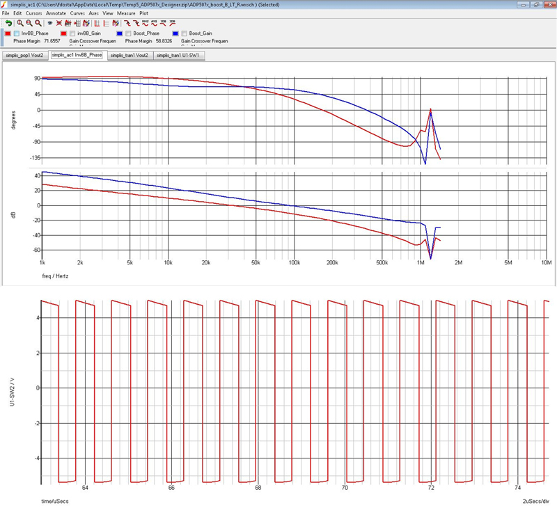
Click image to enlarge
Figure 4. Simulation tool measurement results
Many design tools for switch mode power supplies are available today. They all bring certain benefits. The difficulty is often to understand the offerings of different companies and to understand what a circuit optimizer and simulation tool can and cannot contribute to a switch mode power supply design process.