Innovative Topology Overcomes Conflicting Piezo-Driver Requirements
Piezoelectric elements have traditionally been used primarily in applications in the audio industry, operating in the human audio range (nominally 100 Hz to 18 kHz). However, subsequent improvements in device characteristics have extended their usefulness into markets which demand much-higher performance. For example, nuclear instrumentation and bioscience are among the applications which are pushing the performance of these elements.
Piezo-based actuators are used when a standard electromechanical motor cannot provide the precise, repeatable micromotion needed without complex gearing (and even with gearing, the system would have slop, backlash, and other shortcomings. They are also used to provide motion with extremely fast and precise rise and fall times, such as in ultrasound transducers, as well as for optical-system lens and fixture micropositioning, among other applications. Of course, the piezoelectric principle has also been used for decades in the conventional crystal-based oscillator which generates a clock or tuning frequency in a circuit.
Piezoelectric elements (often referred to as PZTs) can be represented by a series-RC combination, where C can be from several hundred picofarads to several nanofarads, with series resistances between several ohms and one to two kilohms. They can be challenging to drive effectively due to their combination of required voltage levels, sink/source current, and equivalent RC values.
Driving a piezo actuator imposes some unique voltage/current requirements. The drive amplifier for the element must supply high voltage at fast slew rates, and also with precise and repeatable on/off timing. Although a small piezo element looks like a small 1-2 pF load, a larger or multi-element transducer looks like a much-larger load of 100-200 pF, and requires about 50-150 V minimum (and often higher) excitation with a turn-on and turn-off time of several microseconds (and often faster).
As a result, the design needs a relatively high voltage, fast-slewing drive circuit which can source/sink current into a capacitive load, which is very different than what is needed for driving conventional electromagnetic motors.
The design of the PZT drive-circuit problem was especially difficult when a customer's application simultaneously required these stringent piezo-driver specifications for their military project:
Output Specifications:
-Piezo Drive Voltage: ≥350 V (unipolar) or ±75 V (bipolar);
-Load Voltage Slew Rate: ≥4000 V/μsec (min);
-Peak Driving Current: ≥5 A (peak);
-Controlling Bandwidth: ≥10 MHz;
-Gain Flatness to 10 MHz: ≤2 dB. System Specifications:
-Less than ±12 V input;
-PZT element equivalent: 1 nF in series with 30 Ω;
-And, of course, minimum parts count on the bill of materials.
These are challenging requirements, since the specifications appear to be somewhat mutually exclusive: 1. High-voltage operation; 2. High-current output; 3. Wide bandwidth; 4. High slew rate.
It is relatively straightforward to design a system that meets any one of these parameters, but the design then needs to compromise on the other three performance requirements. For example, there are high-voltage (±450 V), low-current (200 mA) op amps, as well as high-current (5 A peak), low-voltage (±200 volts) devices. However, an amplifier with greater than 4000 V/μsec slew rate is currently unavailable in a single op amp, either as a hybrid or monolithic device.
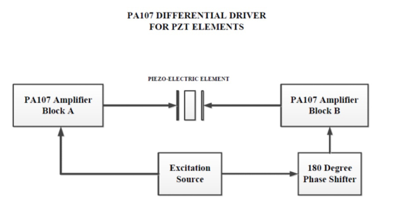
Alternative topology offers a solution
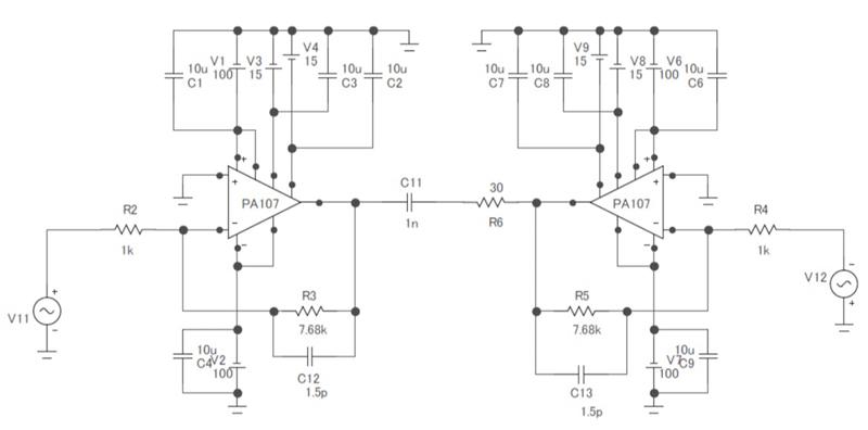
Since there was no conventional approach that would meet the need, it was necessary to investigate the use of a linear push-pull, analog-bridge topology, Figure 1, for the design:
The 1800 phase shifter allows each amplifier to be configured in the same mode of operation; in this case, it is the inverting mode.
Click image to enlarge
Fig 1: One of the useful attributes of the linear push-pull, analog-bridge topology is that it enables the use of identical compensation for each amplifier.
This allows the designer to use identical compensation for each amplifier, since each will be looking into the same load impedance. In contrast, if a single-polarity excitation voltage was used, each amplifier leg would have to be compensated separately, one way for the inverting leg and perhaps another way for the non-inverting leg.
Further, if noise-gain compensation is needed for the inverting leg, another method would be required for the non-inverting side, since noise gain compensation is limited in that configuration. In addition, it is much easier to simply generate a low-voltage complementary-driver voltage.
Note that there are two major advantages when using the linear-bridge circuit, and they enable the design to meet the design criteria:
1. With each leg swinging out of phase with the other, the differential voltage applied to the load is twice that of the output swing of each leg.
2. Measured differentially across the load, the effective slew rate is double that of the single leg.
For this example, the Apex Microtechnology PA107 high-voltage power amplifier was selected as the system amplifier. Its primary specifications include:
1. Slew Rate: ≥2500 V/μsec; 3000 V/μsec (typical);
2. Output Current: 1.5 A (continuous), 5 A peak (within SOA);
3. Gain Bandwidth: 100 MHz at 1 MHz.
Figure 2 shows the Spice simulation circuit developed using Micro-Cap 11 from Spectrum Software, based on using the PA107 in a dual-bridge topology. The PA107 uses ±100 V supplies, and the outputs can swing ±90 V, which is within 10 V of either supply rail. The gain-setting resistors and feedback capacitors were selected based up the gain flatness required at 10 MHz, as well as achieving the required slew rate. (The designer must keep in mind that slew rate is also a function of closed-loop gain.)
Click image to enlarge
Fig 2: The Micro-Cap 11 Spice simulation schematic was critical to performing a full evaluation of the design before any actual prototyping of the design.
During the component-selection cycle, there would be a tradeoff between closed-loop gain, slew rate and bandwidth. The higher the gain, the higher the closed-loop slew rate. However, the higher gain would tend to reduce the closed-loop bandwidth. Conversely, a lower gain would increase the system bandwidth, but reduce slew rate and may approach the ±12-V input needed to drive the complementary outputs to ±90 volts.
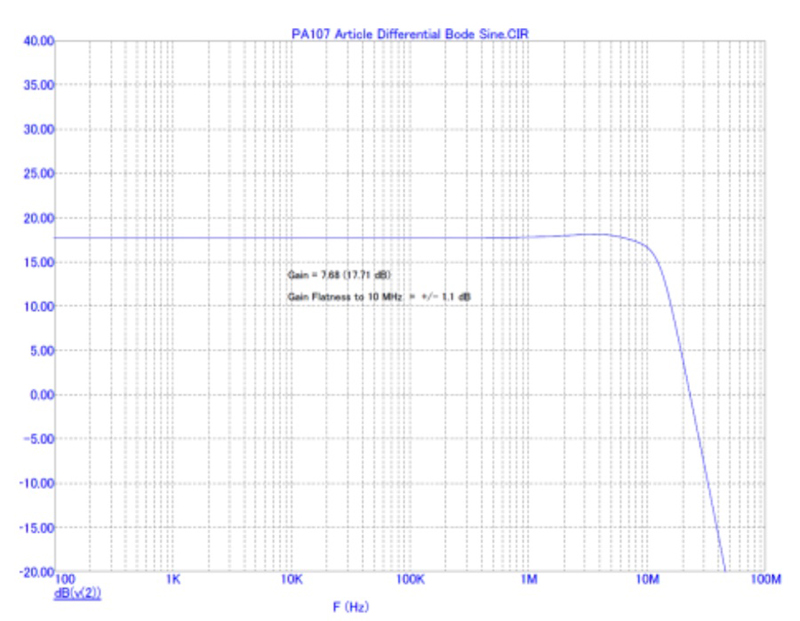
After several iterations and manipulating the values of the feedback resistor and capacitor, the optimal gain was determined to be 7.68 (17.71 dB). This kept the input below the 12-V input threshold and also met the 10-MHz gain-flatness and slew-rate requirements.
Figure 3 shows the simulated closed-loop gain plot of the circuit. Note that the selected gain shows a gain flatness of ±1.1 dB at 10 MHz. The excitation voltage applied to the inputs for the transient analysis was ±11.71 V square wave with a 1 μsec period and a 50% duty cycle.
Click image to enlarge
Fig 3: The simulation of the closed-loop gain of the circuit shows a gain flatness of ±1.1 dB at 10 MHz, at the selected gain.
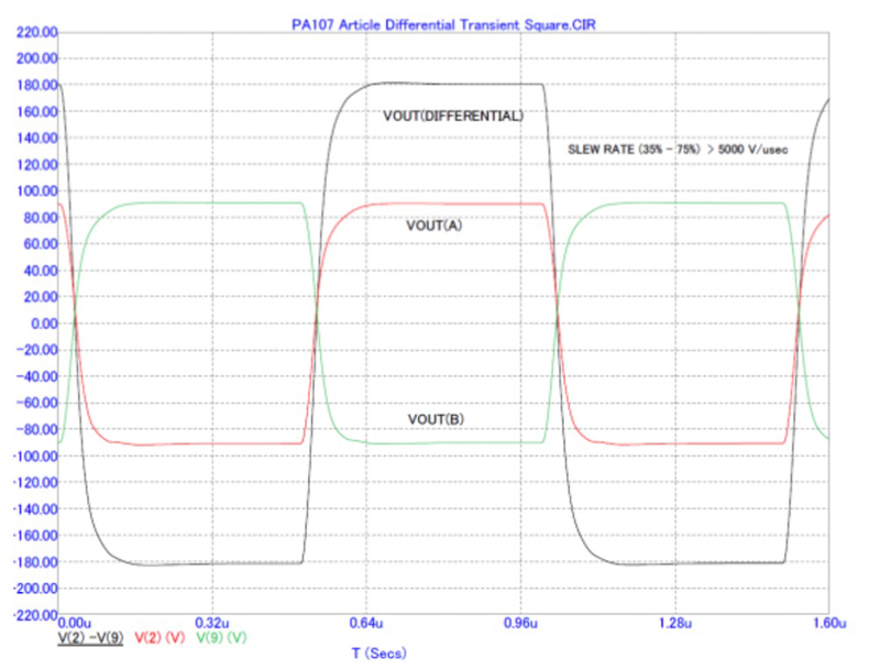
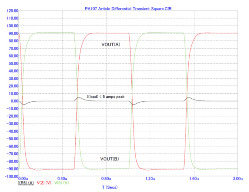
Figure 4 shows the simulations for the output-voltage and slew-rate measurement. The ±90 V output on each leg using ±100-V supplies meant that the circuit could apply 360 Vp-p to the PZT load. The designer does have to consider the peak output current during the transitions where the charge is being transferred across the capacitive element of the PZT. That situation was simulated by looking at the current through R6, Figure 5. The measured current through the resistive element of the piezoelectric element was 4.91 A.
Click image to enlarge
Fig 4: The output-voltage and slew-rate measurement shows 360 Vp-p drive to the load with ±100-V supplies.
Click image to enlarge
Fig 5: The current through R6 indicates the peak output current, which occurs during the transitions where the charge is being transferred across the capacitive element of the PZT.
Results and conclusions
The comparison of the project’s requirements with the simulated results shows the validity of the topology and design approach. By the judicious selection of topologies and components, these very stringent design requirements were met. This result was achieved through the combination of the performance characteristics of the analog-bridge topology and the overall high-performance specifications of the PA107 high-voltage power amplifier.

 PDF
PDF