Author:
Zhongda Li, NPI Manager at UnitedSiC
Date
10/02/2018
 PDF
PDF
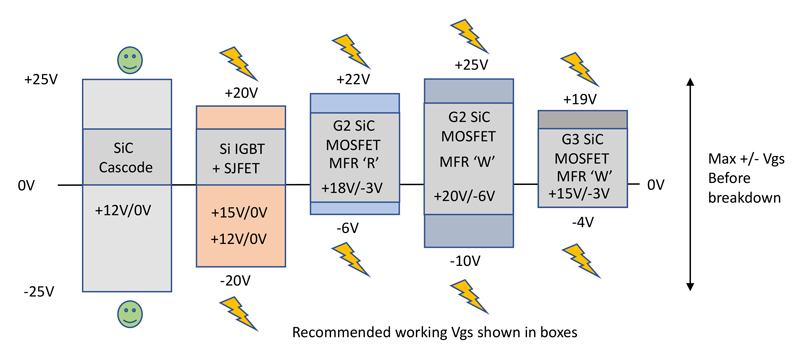
Figure 1. Gate drive voltage comparisons, recommended and absolute maximum
In the days when bipolar transistors were the only option for semiconductor power switches, their base drive circuit was critical for fast and efficient operation. With power device gains often just in double digits, base currents could be huge. Complex arrangements had to be used to drive current in and out at different levels with significant associated power dissipation. The big bugbear was ‘base storage charge’ which slowed switch-off and had to be overcome with negative base voltages and proportional drive circuits or ‘Baker Clamps’. A typical complete base drive circuit might have had 20 passive and active components.
MOSFETs promised easy gate drive
As high voltage, low RDS(ON) Si-MOSFETs became available, gate drive seemed to become easy – just a positive voltage for ON and 0 V for OFF. Power drawn was close to zero at low switching frequencies and all you needed was a series resistor to stop parametric oscillations. Textbooks and application notes made the drive circuits look absurdly simple. Engineers are a skeptical bunch, though, and they soon realized that if you want to use Si-MOSFETs at the high frequencies they are capable of, some effects creep in that make the gate drive more complex to keep efficiency high and prevent failures. The problem is that Si-MOSFETs are far from the ideal switch – they have real input and output capacitance and a ‘Miller’ effect which looks like a variable gate-drain capacitance depending on switching state. They also have non-zero package inductances. Cyclically driving the capacitances around the MOSFET implies power consumption and the Miller effect can allow dangerous spikes of current into the gate ON turn-off, preventing clean and loss-free switching. The source package inductance has a similar effect with high di/dt levels – a voltage is generated opposing the gate drive.
The solution was to choose a positive gate drive voltage for the ON-state for good saturation and a negative voltage for the OFF-state, ensuring that the device is fully OFF when required. Gate drive power is significant, though, proportional to the total gate voltage swing and total gate charge and frequency, with larger devices typically needing several watts. A buffer between control electronics and gate is normally needed to handle the power and peak currents.
Still, Si-MOSFETs are basically voltage-operated devices and the gate drive circuit remains quite simple with good margin achievable between operating and absolute maximum voltage ratings.
Wide band-gap – nice but…
Now, wide band-gap switches in Silicon Carbide (SiC) and Gallium Nitride (GaN) technology are available. The combination of extreme switching speed, low conduction and switching losses, high temperature operation and high voltage has designers reaching for their calculators. How small can the magnetics and other passives be if frequency is increased and can that bulky heat sink be reduced or even eliminated? Spectacular gains in efficiency and size were forecast and demonstrations show real, practical results.
The headline specifications of the new devices are great but the gate drive has now become more critical. Figure 1 shows the recommended drive voltage levels for some SiC MOSFETs and the absolute maximums, which can be frighteningly close; look at the ‘Generation 3’ SiC MOSFET from one supplier, with a recommended negative drive of -3 V and an absolute maximum of -4 V. There is a similar tight margin for the positive recommended and absolute maximum voltage. Designers are rightly worried about reliability with the smallest of transient gate overvoltages. GaN is little better with the latest products needing typically +6 V positive with a +10 V breakdown level.
Wide band-gap devices do have very low total gate charge but the Miller capacitance is still there and non-zero. With potential dV/dt rates upwards of 100 kV/µs, even a few picofarads produce current close to an amp, injected back into the gate drive circuit. Actually, slowing down SiC and GaN devices is usually needed in practical circuits to keep within EMI levels and mitigate the effects of Miller capacitance and package inductance.
There is another solution though; a cascode arrangement of a Si-MOSFET and a normally-ON co-packaged SiC JFET. This combination gives the ease of a MOSFET gate drive with typical absolute maximums of +/-25 V and the speed and low loss advantages of SiC. In a vertical construction, the Miller capacitance is almost immeasurable, at around 1 pF, meaning that a simple 0 V/+12 V gate drive can be used. This makes the gate drive compatible with older Si-MOSFET and IGBT designs, making a drop-in upgrade to SiC in existing systems realistic. You can see the way it compares in Figure 1.
Switching is dramatically fast but can be slowed if needed simply by using a series gate resistor (RG). Figure 2 shows how different RG values control the gate energy EON and dV/dt and di/dt levels for a UnitedSiC UJC1206Kdevice. For fine-tuning of switching speed and EMI a separate resistor can be used for the OFF-drive through an isolating diode.

Click image to enlarge
Figure 2. RG effectively controls switching speed in SiC cascodes
Get that calculator out again
SiC cascodes really do give the best of all worlds with their easy gate drive and robust construction. Do the math with your magnetics and passives using cascodes and see how you can turn miniaturized high-frequency power converters into reality.
UnitedSiC