To minimize system downtime caused by electrical failures, power supplies in high availability systems need protection from overloads and short circuits
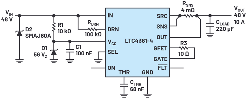
Figure 1. A 48 V, 10 A electronic fuse with an LTC4381
Traditional overcurrent protection (OCP) relies on fuses, but they suffer frombulky size, slow response, wide tolerance, and requiring replacement after one or a few trips. Integrated circuit OCP solutions for DC power supplies, known as electronic circuit breakers or electronic fuses, overcome these fuse disadvantages.
Surge Stopper with Internal Power MOSFET
A surge stopper controls an N-channel power MOSFET placed in the powerpathbetweenaDCpowersupplyand the system electronics needing protection. Built-in output current and output voltage limiting enables a surge stopper to shield load electronics from high voltage input surges and protect the power supply from downstream overloads and short circuits. An adjustable timer activates during voltage or current surge limiting events, allowing continuous system operation for brief fault transients. If the fault persists beyond the timer duration, the system is disconnected from the power supply.
The LTC4381 is the first surge stopper with an internal power MOSFET. It operates with supply voltages up to 72 V while consuming just 6 µA of quiescent current. The internal power MOSFET’s 100 V drain source breakdown voltage (BVDSS) and 9mΩ on resistance (RDS(ON)) allow up to 100 V input surges and 10 A applications. The LTC4381 has four options that offer a choice of fault retry behavior and fixed or adjustable output clamp voltage.
The LTC4381’s surge stopper functionality can be easily extended to work as an electronic fuse. Figure 1 shows the LTC4381-4 in a 48 V, 10 A electronic fuse application, which protects the power supply from an overload or short circuit atthe output. During normal operation, the output VOUT is connected to the supply input VIN through the internal power MOSFET and external sense resistor, RSNS. When the RSNS voltage drop exceeds the 50mV current limit threshold during an output overload or shortcircuit, the TMR pin capacitor voltage starts ramping up from 0V and the internal MOSFET shuts off when the TMR voltage reaches 1.215V (more on this later). The 4mΩ RSNS sets the typical overcurrent threshold to 12.5A (50 mV/4 mΩ) and the minimum threshold to 11.25 A (45 mV/4 mΩ), providing sufficient margin to the 10 A load current.
Due to the parasitic inductance of the trace or cable back to the supply, theinput voltage spikes significantly above the normal operating voltage whenever the internal MOSFET switch is turned off while current is flowing. Zener D1 protects the LTC4381 VCC pin’s 80V absolute maximum rating, while D2 protects the internal 100 V MOSFET from avalanching. D1 also sets the output clamp to 66.5 V (56 V + 10.5 V) in case D2 is not used. R1 and C1 filter VIN spikes and dips. If there is capacitance close to the LTC4381 limiting voltage spikes to below 80 V, then the VCC pin can be directly connected to VIN. In this case D1, D2, R1, and C1 could be eliminated.
With 10 A flowing through the internal MOSFET during normal operation, the LTC4381’s initial voltage drop is 90mV, and power dissipation is 900mW. However, this power dissipation raises the LTC4381 package temperature to about 100°C on a DC2713A-D evaluation board at room temperature ambient, doubling the RDS(ON) and raising the voltage drop to 180 mV. The 4 mΩ sense resistor drops another40 mV at 10 A. More copper area can be spent, especially on the SNS node, to lower the LTC4381 temperature rise. For reference, the DC2713A-D SNS node uses 2.5cm2 of 2oz. copper, spread evenly across the board’s two outer layers.
Start-Up Behavior
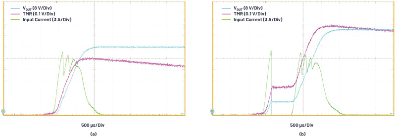
After the ON pin is released from ground, the Figure 1 circuit starts up a 220 µF load capacitor, as shown in Figure 2, for 48V and 60V supplies. 60V is assumed to be the upper limit of the 48 V supply’s operating range. 220 µF is the maximum load capacitor that can be charged up safely by this 10A circuit, assuming no extra load current during startup. If the 220µF capacitor is charged up to 60V at the 12.5A current limit, the inrush time is 220µF × 60V/12.5A = 1.06ms. The LTC4381 MOSFET’s safe operating area (SOA) graph, as shown in Figure 3, reveals that it can survive 12.5 A and 30 V for 1 ms. 30 V is used since it is the average input-to-output differential voltage, which starts at 60 V and ramps down to 0 V.
Click image to enlarge
Figure 2. The LTC4381 10 A fuse circuit starting up a 220 µF load capacitor with (a) 48 V (left) and (b) 60 V (right) supplies
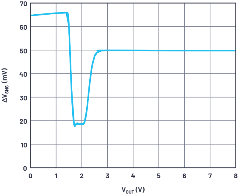
Since there is no GATE pin capacitor to slow down its ramp rate, the output charges up within 2 ms, and the inrush current peaks at 17 A—shooting past the current limit threshold — before being brought under control (see Figure 2). The LTC4381 has a 50 mV current limit sense threshold, or 12.5 A with a 4 mΩ sense resistor when the voltage at the OUT pin is >3V, but it increases to 62mV or 15.5A when the voltage at the OUT pin is <1.5V as shown in Figure 4. This graph also indicates that the output can get stuck at 2 V (and TMR times out) if an electronic load current drops more than 20 mV (5 A for 4 mΩ) across the sense resistor during startup.
Click image to enlarge
Figure 3. The LTC4381 MOSFET’s safe operating area
The waveforms in Figure 2 show that the inrush current pulses instead of being regulated due to the missing 47 nF gate capacitor required for loop stability. In fact, the current shuts off for around 0.5ms during the 60V inrush. The LTC4381 TMR pull-up current is proportional to the power dissipation in the internal MOSFET. Hence, TMR ramps up during start-up inrush even if the current is below the current limit threshold. The gate capacitor has been deliberately omitted to afford a small TMR capacitor that still allows a successful startup for the 220µF load capacitor. A small TMR capacitor protects the MOSFET during a short-circuit fault.
Click image to enlarge
Figure 4. The LTC4381 current limit vs. output voltage
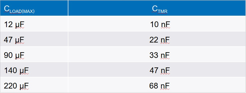
68nF is the smallest TMR capacitor that keeps the TMR voltage rise to around 0.7 V during the 60 V startup. Choosing 47 nF for the TMR capacitor lets TMR reach 1.15 V during a 60 V startup, which is very close to the 1.215 V gate off threshold. A 0.7 V peak TMR target voltage is chosen to provide adequate margin from its 1.215 V gate off threshold while accounting for these tolerances: ±50% for the TMR pull-up current (ITMR(UP) specification in the LTC4381 datasheet), ±10% for the TMR capacitor, and ±3% for the 1.215 V TMR gate off threshold (VTMR(F) specification).
Click image to enlarge
Table 1. Recommended CTMR for CLOAD(MAX)
Table 1 lists the recommended TMR capacitor for a maximum load capacitor to limit the TMR voltage rise to around 0.7 V during a 60 V startup.
Output Short-Circuit Behavior
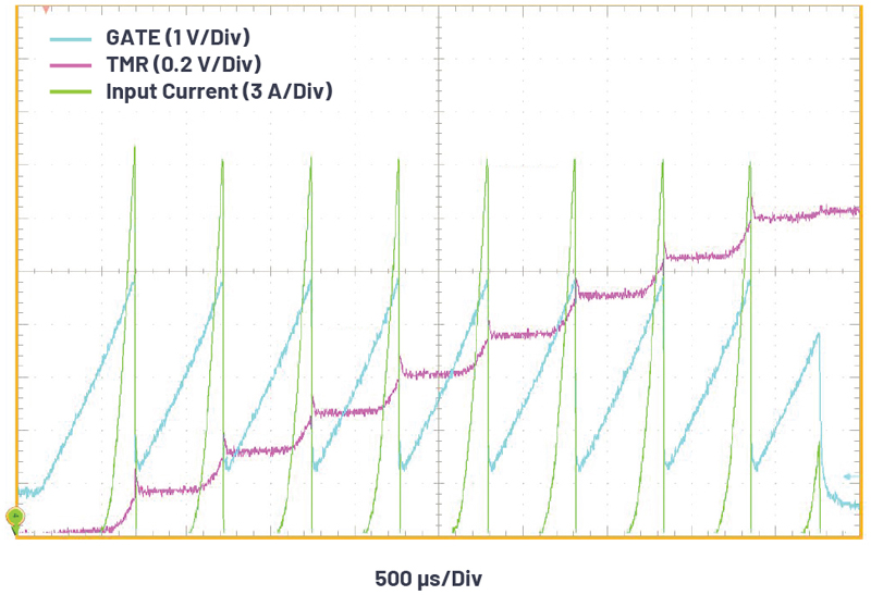
The main purpose of the Figure 1 circuit is to protect the upstream power supply from downstream overcurrent faults, either during startup or normal operation. Figure 5 shows the LTC4381 starting up its MOSFET in the presence of a short circuit at the output. The gate voltage (blue curve) ramps up. When it exceeds the 3 V threshold voltage, the MOSFET turns on, and current (green curve) starts flowing. Due to the output short and the lack of a gate capacitor, the MOSFET current ramps up quickly, exceeding the 15.5 A current limit threshold at 0V output, and peaks at 21A before the LTC4381 reacts to pull down the MOSFET gate and shut off the current flow. The current excursion above 15.5 A lasts for less than 50 µs. Due to the brief power dissipation in the MOSFET, the TMR voltage (red curve) ramps up by about 200 mV. Since TMR is far below the 1.215 V gate off threshold, the gate turns on again, leading toanother spike of current. With each spike of current, the TMR voltage steps up closer to 1.215 V.
Click image to enlarge
Figure 5. The LTC4381 starting up a 48 V supply into an output short circuit
After a few such current spikes, the TMR voltage hits the 1.215 V gate-off threshold and the MOSFET is kept off. The TMR now enters a cool-down cycle, and the LTC4381-4 doesn’t let the MOSFET turn on again until the cool-down cycle completes. For a 68 nF TMR capacitor, the cool-down cycle is 33.3 × 0.068 = 2.3 s long. Since the LTC4381-4 retries automatically, the same pattern of current spikes and cool-down cycle will repeat indefinitely until the output short is removed. An Ltspice simulation does not exhibit the Figure 5 behavior unless 4 µH of input rail inductance is added.


