Elegant step-down conversion for 24V industrial applications
Supply voltage and current monitoring is crucial to concerving power and guaranteering reliability
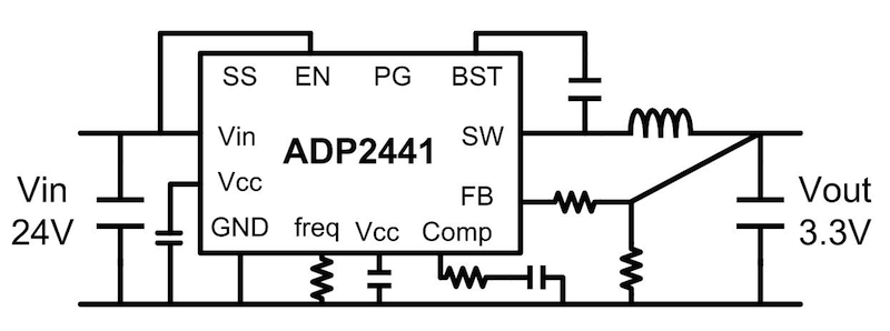
Industrial power supplies need to have very high efficiency today and often times need to be highly compact. In combination with the typical 24V rail available, many solutions utilize a switching regulator rated for 36V Vin max. Unfortunately most solutions available are non-synchronous switching regulators with an external Schottky diode. New synchronous solutions integrating the high side as well as the low side MOSFETs in one chip offer small solution size, high efficiency and especially low switching noise. This article will introduce and discuss a typical 24V down to 5V converter solution with the ADP2441 industrial buck regulator IC. Figure 1 shows the circuit diagram of a 24V to 3.3V step down conversion for industrial applications. In such applications, 24V nominal input voltage usually means that the actual input voltage will me much higher. Typically, plus or minus 20% is quite a common tolerance. Combined with possible input voltage spikes, very often applications demand 36V Vin max. Usually the higher the input voltage capability of a given DC/DC converter the better. Very often, the 24V supply rail is distributed across large factory floors with many different loads attached. Any cable and connector parasitic inductance as well as different loads turning on and off will generate a quite noisy and voltage spike prone environment.
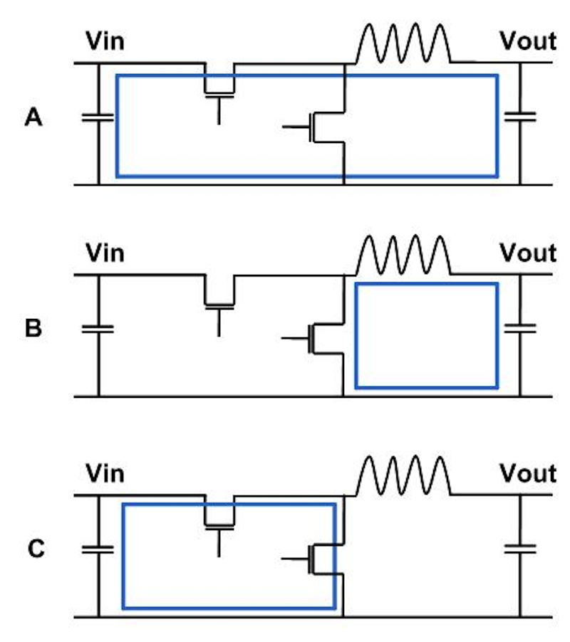
Low EMI, easy board layout It is very elegant not having to worry about an external Schottky diode. After all it is one less component to worry about. Also a low EMI, optimized board layout becomes very simple. Figure 2 A and B shows the current flow in a buck regulator during the on-time and current flow during the off-time of a synchronous buck regulator. Figure 2 C shows the AC-current flow. These are the traces which have to be kept very short and tight to avoid large loops with excessive parasitic inductance which will generate noise. Using a synchronous switching regulator with the high side and the low side switch integrated, the trace between the high side and low side switch stays all internal on the die. This AC trace will not need to go through bonding wires, IC package pins and board traces with quite high parasitic inductance. This AC trace is kept local with low parasitic inductance and thus very low EMI. The only trace the design engineer needs to worry about is the connection traces of the input capacitor. It needs to be places as close as possible to the Vin and ground pins of the IC. This is a simple task and thus board layout is very easy. Very good EMI behavior can be achieved this way. High efficiency Synchronous switching regulators (two active switches instead of one active switch and one diode) are usually more efficient than non-synchronous regulators. This efficiency advantage becomes significant as the output voltage becomes lower and lower in newer applications. The voltage drop across a diode of about 0.6V versus the voltage drop across a fully turned on MOSFET (0.2V as an example) is higher. When looking at an output voltage of 12V, this voltage drop difference is not so significant. When dealing with output voltages of 2.5V or 1.8V however, the voltage drop across the low side switching element becomes quite important for the overall efficiency. Five years ago, most industrial applications powered off a 24V bus, required a 5V system voltage for some function. Today, we see applications where the highest system voltage is 3.3V or even 2.5V. For these systems, the efficiency advantage of using a synchronous switching regulator becomes greater. High switching frequencies Designing a power supply with high switching frequencies increases switching losses and thus decreases the overall efficiency in most cases. However, some applications call for low solution cost as well as small solution size. These demands yield the utilization of a high switching frequency in order to save space and cost of the inductor and capacitors used. The ADP2441 has an adjustable switching frequency of up to 1MHz. The ADP2442 is very similar to the ADP2441 but the switching frequency can also be synchronized to a clock frequency of up to 1MHz. While 1MHz is not so unusual for a switching regulator, there is an important limitation which many available devices on the maket have. It is the minimum on-time. This is a time period that the switching regulator keeps the high side switch turned on before it can turn it back off. While at low frequencies, the minimum on-time does not matter much, at higher switching frequencies this is a very important specification. At 1MHz switching frequency, there is 1000ns in one cycle. When stepping down 24V to 2.5V, the duty-cycle would need to be roughly 10%. So the switching regulator needs to turn on the high side switch for 100ns. If the nominal 24V happens to be a bit higher for a certain amount if time, the on-time will reduce to periods shorter than 100ns. Many 36V switching regulators on the market have a minimum on-time of higher than 150ns and in many cases the minimum on-time is not even specified. Circuit designers then notice that the regulator is skipping switching cycles and that the switching frequency is not fixed at 1MHz anymore. The ADP2441 was designed for high switching frequencies at large step-down ratios. It has a specified minimum on-time at 50ns typical and 65ns is guaranteed as a worst case value. This allows the design of step-down switching converters at 1MHz from a high input voltage to very low output voltages.
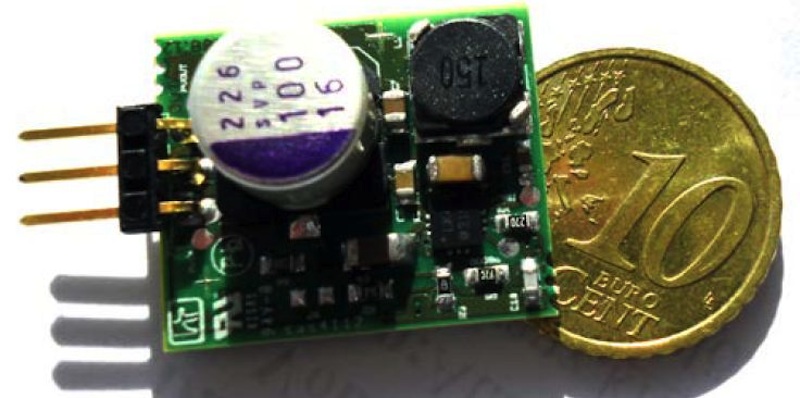
Circuit example and design tools Figure 3 shows a circuit stepping 24V industrial bus voltage down to 5V. It is operating at 500kHz which is a good compromise between high efficiency small solution size and low component cost. The board was designed by the franchised German Distributor Semitron to be used as a replacement for 24V to 5V TO-220 packaged linear regulators which are still in place in many low current industrial applications today.
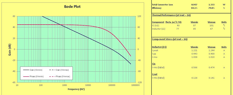
For design engineers there is a circuit design tool available which can help to select external components and circuit parameters such as switching frequency very quickly. The tool is able to select the right external components from a passive components database to suit complex operating conditions. The user can enter a certain expected load change on the output and the amount of output voltage overshoot or undershoot which is acceptable. Then the tool will select the right type of output filter to accommodate these requirements. Stability considerations can be evaluated with the integrated Bode plot section. The tool can be downloaded free of charge from the product folder of the ADP2441 on the Analog Devices website. Analog Devices