Introducing a chipset that enables the use of non-complementary clamping solutions and the design of super-dense flyback power supplies.
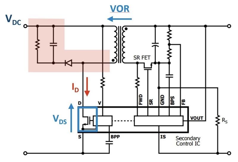
Figure 1: A passive primary clamp RCD solution (highlighted) is highly dissipative and limits the efficiency and operating frequency of flyback power supplies
Off-line flyback power supplies require a clamp circuit (sometimes called a snubber) on the primary side of the transformer to limit the drain-source voltage stress on the power MOSFET when this switch turns off during normal operation. There are several approaches to designing these clamp circuits. Low-cost passive networks are effective but must dissipate the clamp energy each cycle, reducing efficiency. Active clamps employing complementary drive techniques for the clamp and power switch are an improvement and can be much more energy efficient, but they impose operating limitations on the power supply’s operating modes (no CCM operation, for example). A more advanced control technique – non-complementary active clamping – ensures the most cost-effective use of clamp energy and avoids the design limitations imposed by complementary active clamp circuits.
In a flyback converter, voltage (VOR) is reflected from secondary side when the primary side switch is turned off and the stored energy is transferred to the load through transformer (Figure 1). VOR is amplified by the transformer turns-ratio and adds to the voltage stress on the switching device imposed by the VDC input rails. In conventional circuits, a passive primary clamp is added to limit this voltage excursion.
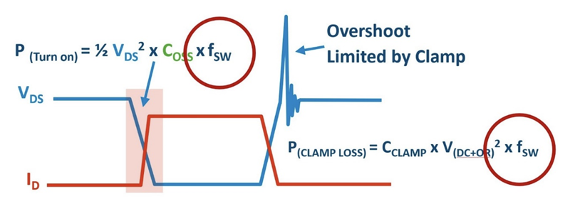
In addition to voltage stress (VIN + VOR), there is a large voltage overshoot at turn-off caused by the stored energy in the leakage inductance of the primary winding. The clamp limits the voltage overshoot caused by these three elements and protect the primary switch (Figure 2). In addition, with this circuit configuration, the power switch turns on when the drain voltage is high. Switching loss is proportional to VDS2, so a high VDS increases turn-on losses in the switch, further decreasing efficiency.
Click image to enlarge
Figure 2: Turn-on losses and clamp losses are both related to switching frequency
The clamp capacitor absorbs the leakage-inductance energy, but that energy is then dissipated by the clamp resistor. Energy is lost during every switching cycle, limiting the switching frequency in practical designs. Lower switching frequencies require larger transformers. So, the use of a passive clamp increases losses and reduces switching frequencies, both of which contribute to larger power supplies. An active clamp can be used to address those limitations.
Complementary active clamps
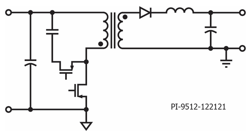
An active clamp replaces the resistor in an RCD clamp with a switch, usually a power MOSFET (Figure 3). Instead of dissipating the leakage inductance energy, it recycles the energy back to the transformer. In a complementary active clamp, the clamping switch is turned on when the main MOSFET is turned off, with a small amount of deadtime inserted between these events. The clamp capacitor gets charged, and just before the main MOSFET turns on, the clamp switch is turned off and the energy in the clamp capacitor is recirculated to the output. This active clamp is called a complementary drive scheme, because the main MOSFET and the active clamp switch act in a complementary fashion.
Click image to enlarge
Figure 3: Simplified schematic of a typical [complementary] active clamp implementation
Zero voltage switching can be implemented using sophisticated adaptive control techniques to achieve resonance between the leakage inductance and clamp capacitor. The leakage inductance resonates with the clamp capacitor when the clamp switch turns off in order to discharge the power MOSFET’s COSS prior to turning on, resulting in zero-voltage switching. The resonant action will be rendered ineffective by a high output capacitance (reflected to the primary via transformer action adding to the clamp capacitance). There is insufficient leakage energy available in a typical transformer to accommodate this capacitance. To overcome this, a two-stage LC filter is required to both ensure a low value primary capacitance and meet output ripple requirements. This complementary active clamp solution is an improvement over a passive clamp, but still has limitations including:
1. The need to use burst mode at light load, which results in higher output ripple
2. Two-stage output filter
3. Limited to critical conduction mode or discontinuous conduction mode (CrM and DCM); no CCM operation makes wide-output USB PD designs difficult to implement
Increased performance with non-complementary active clamping
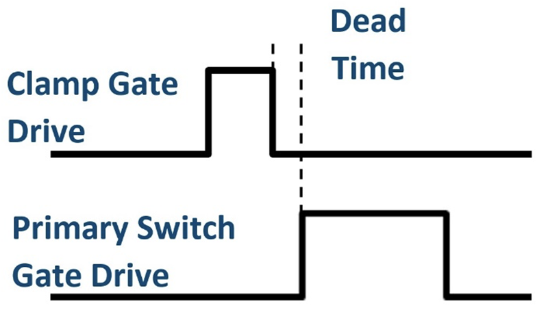
With non-complementary control, instead of turning the clamp switch on shortly after the main MOSFET is turned off, the clamp switch is turned on for a short period just before the main MOSFET turns on. Non-complementary control is able to operate in continuous conduction mode, as well as discontinuous conduction mode (and CrM), and still implement zero voltage switching. That enables the design of power supplies that have very wide input voltage ranges, as well as large output voltage ranges which are needed when designing efficient USB PD chargers. With conventional control schemes, the synchronization of the non-complementary clamp drive with primary and synchronous rectification switching can be challenging. The adoption of a single controller to manage the switching of all three devices greatly simplifies the circuit and ensures reliable operation.
Click image to enlarge
Figure 4: With non-complementary mode switching, the active clamp is cycled just before the primary switch
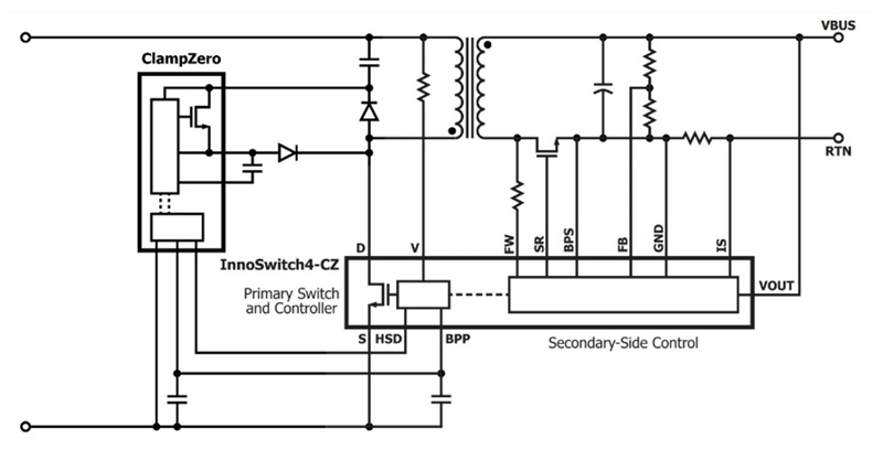
Non-complementary active clamp control can be implemented using the Innoswitch4-CZ / ClampZero chipset from Power Integrations (Figure 5). InnoSwitch4-CZ devices feature a robust PowiGaN 750 V switch, secondary controller directing operation of the main switch, clamp switch and the synchronous MOSFET, and an internal safety-rated control link – FluxLink, in a single InSOP-24D package. InnoSwitch4-CZ ICs include two pins dedicated to the non-complementary control of the ClampZero active clamp; the high-side drive (HSD) pin to turn the ClampZero on and off, and the V pin for measuring the DC rail voltage.
Click image to enlarge
Figure 5: InnoSwitch4-CZ with HSD signal to control switching of the ClampZero active clamp and the V pin that senses high line conditions and enables the use of discontinuous mode
The secondary-side controller sends the command that initiates the HSD signal to turn the ClampZero PowiGaN switch on in order to resonate the leakage inductance and clamp capacitor before the commutation of the primary PowiGaN switch. There is a very small amount of delay between the turn-off of the ClampZero device and turn-on of the main switch, which is externally programmable using a small resistor on the HSD pin to help optimize timing.
For continuous conduction mode, the HSD signal is on for one quarter of the resonant period caused by the leakage inductance operating with the clamp capacitor. A challenge with using this mode of resonance for wide range operation is that the leakage inductance is typically a very small value and the amount of energy needed to achieve zero voltage switching for high line increases when the voltage across this MOSFET is increased. That’s where discontinuous mode control comes in.
For discontinuous mode (high line operation), the HSD signal pulse width becomes one quarter of resonance between the magnetizing inductance (plus leakage inductance though leakage inductance is typically a very small component co pared to magnetizing inductance), and the clamp capacitor value. The V pin line voltage information is used to control initiation of discontinuous mode. When a high-line condition is sensed, the delay between ending the ClampZero drive and turning on the main switch is also increased. That enables more time for the resonance between the magnetizing inductance (and leakage inductance) and the clamp capacitance to bring down the voltage on the power switch. This mode of operation does not require the burst mode required for complementary active clamp circuits avoiding the risks of higher output ripple and audible noise experienced with complementary mode circuits.