Ensuring SoC Power Integrity with Silicon Capacitors

Embedded high density silicon capacitors enable sub-5pH ESL
Figure 1: MLCCs and parasitic impedances cause PDN impedance responses to deviate from their target.
In the relentless pursuit of high-performance computing, power delivery has quickly become the industry’s greatest roadblock. As artificial intelligence (AI) and high-performance computing (HPC) drive an exponential increase in current densities and transient requirements, traditional power delivery networks (PDNs) are falling short.
For decades, the industry has relied on multi-layer ceramic capacitors (MLCCs) to decouple systems from load transients. But as load currents and frequencies skyrocket, MLCC’s relatively high parasitic inductance is starting to limit performance. For the industry to deliver the stable power that AI and HPC need, we must embrace a new direction for decoupling.
Fortunately, silicon capacitors offer a way forward.
Bottlenecks in Modern PDNs
A stable power supply is the backbone of any system-on-chip (SoC). Ideally, a PDN should maintain a perfectly flat, low impedance across all operating frequencies to ensure that sudden bursts of processor activity do not cause voltage instability. But, in reality, every physical connection between the voltage regulator and the compute die – including board traces, package vias, and solder bumps – introduces parasitic inductance and resistance.
To counteract these effects, designers have historically relied on a staggered network of capacitors to decouple the system from high-frequency load transients. The strategy involves using multiple capacitors of varying case sizes in parallel to flatten the impedance across the spectrum. Thus far, the MLCC has been the component of choice to achieve this end. But, despite their long-standing status as the industry workhorse, MLCCs have a fundamental flaw in the form of high equivalent series inductance (ESL).
As modern workloads push switching frequencies into the tens to hundreds of megahertz range, the aggregate ESL interacts with the rest of the PDN in undesirable ways. One example is impedance peaking, where the parasitic inductance reacts with the surrounding network to create sharp resonance spikes as illustrated in the example PDN and impedance plot in Figure 1. In this example, the group of MLCCs, even though embedded in the package substrate, still result in a resonance peak in the 6-20 MHz range. When a processor's workload coincides with these frequencies, the resulting impedance spikes trigger significant voltage noise and deep power droops.
To prevent these fluctuations from causing logic errors or system crashes, engineers will often implement voltage margining, which involves setting the nominal supply voltage higher than requirements to keep it above the minimum threshold during transient events. This practice is inherently wasteful, as it increases the chip's overall power consumption and generates excess heat.
Silicon Capacitors: A Semiconductor Approach to Passives
Just a few silicon capacitors are the solution.
Semiconductor foundries can manufacture silicon capacitors using the same high-precision lithography and etching tools as those used for advanced integrated circuits. By etching deep, high-density 3D micro-trench structures into silicon wafers, manufacturers can achieve large capacitance surface areas with an incredibly small, thin footprint. This process allows for capacitance densities exceeding 2 uF/mm2 today, with future targets climbing even higher (Figure 2).
Click image to enlarge
Figure 2: Device structure of a silicon capacitor.
By fundamentally altering the component’s electrical and physical characteristics, silicon capacitors provide several notable technical advantages over ceramic alternatives.
One of the most significant benefits is that they provide orders-of-magnitude lower ESL (often less than 10 pH), which allows them to counteract high-frequency impedance peaks and achieve a much flatter PDN. And, while traditional MLCCs can lose significant effective capacitance due to temperature fluctuations or DC bias, silicon-based devices are ultra-stable across a wide operating envelope (Figure 3).
Click image to enlarge
Figure 3: Silicon capacitors offer better stability over DC bias than MLCC-based alternatives.
From a design perspective, compatibility with IC packaging tools means that designers can achieve thousands of terminals and pad pitches as fine as 100 microns (µm), a level of precision that perfectly matches the processor’s pinout. The semiconductor manufacturing process also delivers µm-level precision in X-Y dimensions and die thickness to ensure a perfect fit within advanced, high-density substrates. Similarly, the monolithic silicon structure unlocks sophisticated multi-terminal components that further minimize the mounting inductance between the capacitor and the die.
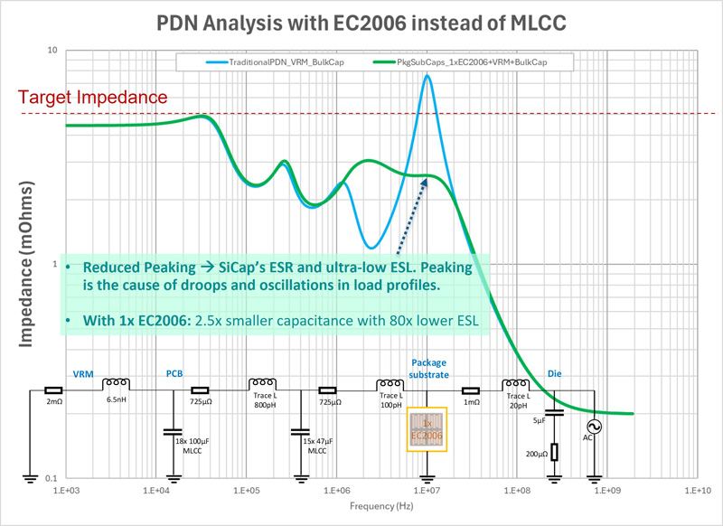
Figure 4 illustrates the effect of replacing the MLCC bank in the package with a single monolithic silicon capacitor device in the same PDN as Figure 1. The resonance peak previously observed is flattened with a 3x reduction, driving a much more predictable and flat noise profile in the same 6-20MHz range. Interestingly, the silicon capacitor used in this example is 2.5x smaller in capacitance but also 80x lower ESL, being the key factor in flattening the PDN.
Click image to enlarge
Figure 4: Embedded silicon capacitor replaces the MLCC bank in the package.
Placing Power Decoupling Where It Matters
The most impactful aspect of silicon capacitors is where designers can place them. Because they can be manufactured as thin as 40 to 50µm, or roughly half the thickness of a human hair, designers can integrate them directly into the processor package. This ultra-thin profile, combined with tight tolerances on X-Y dimensions and die thickness, allows designers to move decoupling capacitance away from traditional distant PCB locations and integrate it directly into the processor package (Figure 5).
Click image to enlarge
Figure 5: Mounting options for silicon capacitors.
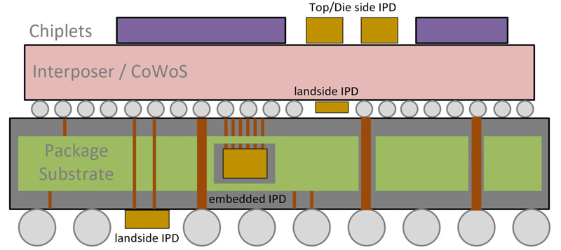
Engineers currently use three high-impact locations to maximize power integrity, as shown in Figure 6.
Landside Mounting
In this configuration, engineers mount silicon capacitors on the bottom (landside) of the package substrate. By thinning the capacitors to approximately 75µm, they can sit entirely within the height of the ball grid array (BGA) solder balls. This proximity to the SoC significantly reduces the physical path current must travel compared to board-level MLCCs. In a recent case study involving a mobile SoC (the Xiaomi 15s Pro), 75µm thick silicon capacitors were mounted landside to achieve a 6x reduction in ESL compared to a standard MLCC solution.
Substrate Embedding
Embedding is state-of-the-art for high-performance AI accelerators. Here, manufacturers create a cavity 400 to 750µm thick in the package substrate and place the silicon capacitor inside. This placement enables a direct vertical connection between the die and the capacitor via laser-drilled vias and copper pads. Placing the capacitor directly beneath the die and matching the xPU’s pinout reduces the mounting inductance to near zero, resulting in the most efficient path for high-frequency energy delivery.
Click image to enlarge
Figure 6: Silicon capacitor mounting options include landside, interposer landside, and embedded in the substrate.
Interposer Landside
For advanced 2.5D and 3D chiplet architectures, designers can integrate silicon capacitors on the landside of the silicon interposer. This approach requires the most extreme thinning, often reaching 40-50µm, to fit between the interposer and the package substrate. Disaggregated IP designs benefit, as landside placement provides localized, high-frequency filtering as close as possible to the individual die or chiplets.
By moving the decoupling capacitance into these creative locations, designers can optimize the PDN for the lowest possible mounting impedance.
Efficiency and Performance in the Real World
By moving from a bank of MLCCs to a single silicon capacitor, designers can realize tangible system gains.
In HPC environments, silicon capacitors help reduce voltage noise and deep power droops associated with impedance peaking. With greater baseline power integrity, designers can significantly reduce their supply voltage, as they no longer need to maintain high voltage margins to protect against transient-induced logic errors. A reduction of just 50 mV in supply voltage can translate to approximately 13% in total power savings for a high-performance compute die. These energy savings directly lower operating costs and reduce the system's heat signature.
Alternatively, designers can leverage this improved thermal and power headroom to push performance boundaries rather than just saving energy. By maintaining a stable supply under heavier loads, the processor can run at a higher thermal design current (TDC), which enables higher utilization and faster clock frequencies within the same thermal envelope.
Delivering the Future of Power
As the industry embraces disaggregated chiplet architectures and higher current densities, the limitations of traditional passive components are no longer tenable. Silicon capacitors are a novel approach that brings the precision and performance of semiconductor manufacturing to the world of power integrity.
Empower Semiconductor is leading this charge, offering the highest-density and lowest-proven-impedance silicon capacitor solutions currently qualified for high-volume production. By supercharging SoC power integrity, silicon capacitors are ushering in the next generation of AI and HPC performance.