For special applications or migration to CMOS capabilities
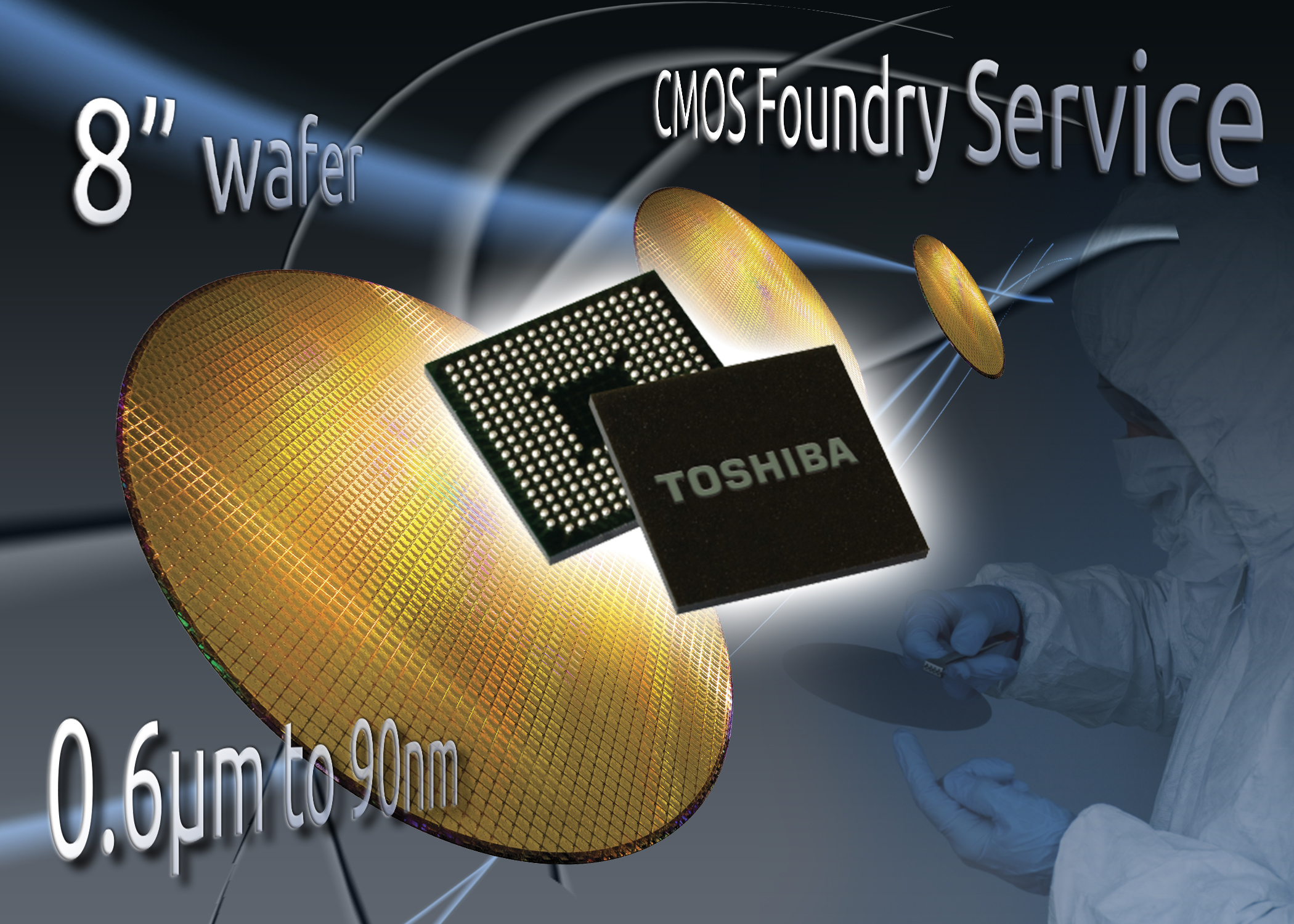
Toshiba offers European customers process development and fabrication services on 8" wafers at 600, 350, 180, 130, 110, and 90 nm process nodes.
Toshiba Electronics Europe is now offering European ASIC customers a flexible process-development and foundry service built around its 8" CMOS fabrication capabilities. The service combines support for special processes, process modifications, and process development with cost-effective medium- and high-volume manufacturing backed by a commitment to long-term supply. Toshiba's service is for customers developing special applications including sensors, detectors, and other analogue functions and for companies looking to migrate existing applications to commercially-attractive CMOS-based technology. Currently available process nodes comprise 600, 350, 180, 130, 110, and 90 nm. Standard IP options range from logic and embedded memory (SRAM, ROM, EEPROM, and Flash EEPROM) to CMOS sensors. High-voltage CMOS and DMOS processes are also available. Working closely with Toshiba development teams, customers have the flexibility to define a range of options, devices, design rules, and modules. These include special wafer substrates, custom-specific process modules, special implant- and diffusion-process conditions, and custom layer stacks. Toshiba is also offering non-standard post-processing steps such as through-silicon-vias, protection films, optical films, and micro-lenses. The flexible process foundry service also covers wafer probing and light/dark testing in Toshiba's fab in Iwate, Japan. This facility is fully certified in accordance with ISO14001, TS16949 and OHSAS18001. Toshiba components Toshiba foundry services deeplink