Key changes have come to pass that can change the way we use GaN devices
When I started working with eGaN FETs almost six years ago, I had no idea what to expect from this technology. We had our first preliminary datasheet and even though I had no idea what to expect, it was obvious that, on paper, these devices were much better than your typical MOSFETs – already beyond the theoretical silicon limit.
Since then, many improvements have been made to both the devices and to the overall structure of the power conversion stage of which they make such an integral part. This article will discuss some of the key changes that have come to pass, as well as the impact they have had on the way we use GaN devices and applications that have been enabled through their existence.
From a simple beginning
EPC’s very first part, the EPC1001, was an enhancement-mode GaN FET. It was a 7 mOhm (max), 100 V device that exemplified the strategy of developing products that looked and behaved just like enhancement-mode power MOSFETs. The choice of using a wafer level chip-scale package (WLCSP) came just as much out of necessity, as it did out of realizing the limitations that packaging has on device performance. Having a high voltage lateral device allowed all three terminals of the FET to be directly connected to the PCB, thus removing the need for two-sided packaging that not only increases a device’s parasitic inductance, but increases the overall cost and thermal impedance as well.
Device improvement
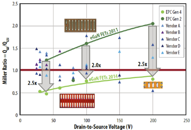
The initial offering of the device was in two sizes and spanned a voltage range from 40 V to 200 V. Over the next five years, a large number of device improvements have been made. The first major course of action, improving the Miller charge ratio (QGD/QGS1) to below one, was achieved on the ultra-high frequency EPC8000 series products and has been maintained for all subsequent parts, as shown in Figure. 1. This achievement is significant, as a ratio of less than one for the Miller charge ratio will guarantee theoretical dv/dt immunity [6]. The products in the EPC8000 series also have a pad layout with a separate gate-return connection that minimizes the common source inductance. These products are ideally suited for multi-megahertz hard-switching operation.
Click image to enlarge
Figure 1. Miller Ratio (QGD / QGS1) comparison between current and initial eGaN FETs relative to state-of-the-art MOSFETs
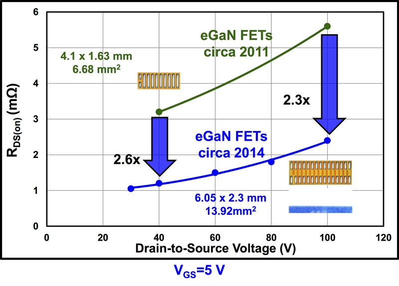
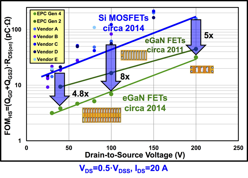
The next major improvement was the creation of our fourth generation parts that resulted in a significant increase in maximum die size as shown in Figure 2. These products also extended the voltage range down to 30V, with a 1 mOhm (typical) on-resistance. At the same time, the new footprint of these devices was created with a ‘slot’ along the center of the die, which allowed for the placement of PCB vias directly under the die. This location minimizes the impact of PCB busing. As shown in Figure 3, the improvements in Miller ratio translated into improved Figures of Merit (FOMs) for these devices.
Click image to enlarge
Figure 2. Minimum on-resistance (RDS(on)) vs. maximum drain-to-source voltage improvement over time
Click image to enlarge
Figure 3. Hard-switching FOMHS comparison of eGaN FETs and state-of-the-art Si MOSFETs showing improvement over time
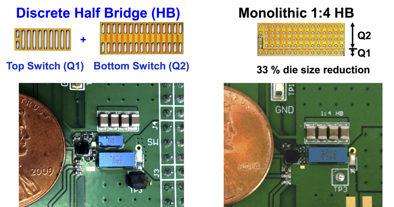
Probably the most important development that followed these improvements was the monolithic integration of multiple devices capable of voltage isolation between them. The flagship product, the EPC2100, allowed the creation of devices with high aspect ratios, which are not practical as discrete devices (see Figure 4). This not only lowered overall power-loop inductance to below 200 pH, but improved thermal performance of the smaller device with the addition of a lateral thermal path through the larger and cooler neighboring device. Considered the world’s fastest power switches, they are capable of switching 12V at 20A with voltage rise times under 700ps.
Click image to enlarge
Figure 4: Implementation of eGaN FET-based half bridges with discrete transistors (left) and an integrated monolithic GaN IC (right)
Following the introduction of these products, further levels of integration, up to three devices, and expansion into higher voltage up to 450 V, have been made. Most recently, overall advances in device performance have allowed the creation of wider-pitch connection parts. These products are coined ‘Relaxed Pitch’ and have a 1 mm pitch between pins that are suitable for high copper ounce thickness PCBs. The device developments are only one side of the story; in parallel, a number of key power system changes have been made.
System changes
Although our initial intentions were to develop direct replacements for existing MOSFET devices, it was quickly realized that significant system-level changes would be required to extract the most value out of these new high performance devices. In an effort to share our experience with our customer base to these requirements, we published our first text book, GaN Transistors for Efficient Power Conversion, on how to best use GaN transistors for power conversion.
We continued to share our experience with the publication of a second edition of our textbook. Apart from addressing the gate driver requirements of the eGaN FETs and minimizing common source inductance through layout, the development of a more ‘optimum’ power loop within the PCB was required. Unlike with traditional MOSFET packages, the parasitic inductance of the PCB dominates the overall loop inductance when using high performance eGaN devices.
A unique characteristic of eGaN FETs is that they do not exhibit any ‘body’ diode reverse-recovery. This results in the diode reverse recovery of the bootstrap supply diode becoming a bottleneck at multi megahertz switching frequency, which cannot readily be addressed with silicon devices. The solution to this limitation came by using eGaN FETs themselves as synchronously-switched bootstrap diodes. This, in turn, led to the synchronous bootstrap diode being integrated within a monolithic eGaN integrated circuit for high frequency half-bridge applications.
Enabled applications
The multi-pronged approach of developing superior performance power FETs using GaN, while simultaneously reducing the parasitics inherent with both device packaging and PCB, resulted in circuit performance that is unmatched by silicon MOSFETs. The benefit is that a number of key applications are being enabled through the use of eGaN FETs, for example:
LiDAR (Light Detection And Ranging)
The use of LiDAR for spatial mapping is not new, the improved resolution systems make this technology suitable for virtual reality gaming and autonomous vehicles. Both of these applications require the generation of multiple ampere current pulses with durations of only a few nano seconds. GaN offers improvements in both edge rate and peak amplitude, which directly impact LiDAR performance.
Envelope Tracking (ET) for Cellular Base Stations
Modulating the supply voltage of the Radio Frequency Power Amplifier (RFPA) by tracking the RF envelope has been successfully developed for cell phones to improve battery life. Achieving the same for the much higher power and voltage levels of base stations are not possible with silicon, but the potential to reduce an ever-growing information and communications technology (ICT) energy consumption by reducing the RFPA losses by up to two-thirds is vital for addressing global energy consumption. With eGaN FETs, envelope tracking supply efficiencies of over 92% at power levels up to 120 W to 4G LTE bandwidths are now possible.
Wireless power transfer
The drive for wireless power transfer with spatial freedom, such as the standard championed by the Alliance for Wireless Power (Rezence) that requires multi-megahertz switching amplifiers at ever-increasing power levels. The use of eGaN FETs not only enables these higher power levels, but also allows multi-mode compatibility using a single amplifier.
Looking forward
The combination of lower on-resistance, faster switching speeds, lower thermal impedance, and smaller physical size of eGaN FETs continues to raise the bar for power transistor performance. As GaN technology matures, not only does the performance of these transistors rapidly improve, but significant reductions in cost are also realized. Not only will GaN devices continue to enable new applications, they will replace silicon power transistors in cost-sensitive applications as well. As a matter of fact, the first signs of this happening are already here.